Inkjet Printing for Solar Cell Manufacturing: How Electroforming is empowering the photovoltaics industry moving forward
Inkjet printing is an extremely versatile, non-contact process that involves jetting tiny ink droplets to facilitate direct printing. It has seen a surge of new applications in fields including electronics, life science, optics, and PV.
inkjet printing for solar cell manufacturing
The demand for energy transition is constantly increasing, especially since the Paris Agreement stipulates that the world must become greenhouse gas neutral by the second half of the century to limit the increase of global temperatures to a maximum of 2°C. Solar power plays a vital role in energy transition and climate protection as it affords a drastic reduction in greenhouse gasses, which arise through the burning of fossil-based fuels such as oils, coal, and gas.
In this context, accumulated research and effort have been taken to improve the efficiency of solar power. Crystalline silicon (Si) photovoltaic (PV) cells are the most common solar cells used in commercially available solar panels. They have dominated the PV cell market since its early beginnings, around the 1950s, and account for more than 90 percent of it today.
The outlook for higher efficiency in photovoltaic cell manufacturing — from better screens to no screens
A large number of PV cell manufacturing companies and research institutes have been devoted to improving cell efficiency and reducing costs to develop high-efficiency crystalline Si PV cells. An essential step in producing these cells is the metallization process of creating a grid of very fine lines on the front side of the wafer that conduct the light-generated electrons away from the cell.
This metallization process is most often undertaken using screen printing technology, whereby conductive paste is forced through the openings of a wire mesh or emulsion screen onto the wafer to form the circuits or contacts. Over the years, efforts to improve the efficiency and precision of PV cell metallization have led to better screen printing equipment and materials. For example, high-precision stencils have been introduced as an alternative to traditional wire mesh and emulsion screens. Moreover, the development of inkjet printing and 3D metal printing technologies has allowed for the realization of maskless screen printing.
(1) Screen printing
The screen printing process begins with a Si wafer being placed on a printing table. A screen, usually a wire mesh or emulsion screen, is mounted within a frame and placed over the wafer. This screen blocks certain areas and leaves other areas open. Metal paste, usually silver (Ag), is then dispensed onto the screen using a squeegee so that it is spread uniformly to fill the screen openings. As the squeegee moves across the screen, it pushes the paste through the openings, transferring it onto the wafer.
A grid of conductive circuit lines is deposited this way. These thin and delicate lines, also referred to as fingers, collect and conduct the light-generated electricity from the active regions to larger collecting lines, or busbars, and then to the module’s electrical system.
However, the lines are not as thin as desired, since they block sunlight from reaching active parts of the cell and thus reduce conversion efficiency. To minimize this so-called shadowing effect, efforts have been made to make the lines as narrow as possible as well as taller to maintain the same cross-section for adequate conductivity. (image 1)
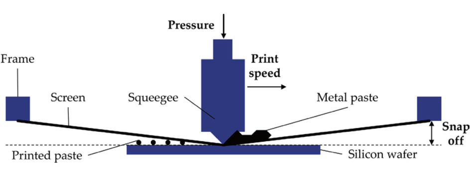
image 1. screen printing process
(2) Stencil printing
The stencil printing process was introduced after the screen printing process. The development of high-precision metal manufacturing technologies such as electroforming meant that high-precision stencils became an alternative for achieving achieve finer, taller contacts in PV cell manufacturing. As in screen printing, these stencils, with blocked and open areas, are used to apply the paste to the wafer.
Stencil printing overcomes the limitations of screen printing in aspect ratio (i.e. line height/line width), finger width, and uniformity. The much finer lines with higher aspect ratio and better durability. All of these in the end lead to much higher yields and lower costs. Lab tests have shown stencil printing as offering a 0.25 percent PV cell efficiency improvement over screen printing. (image 2)
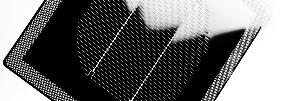
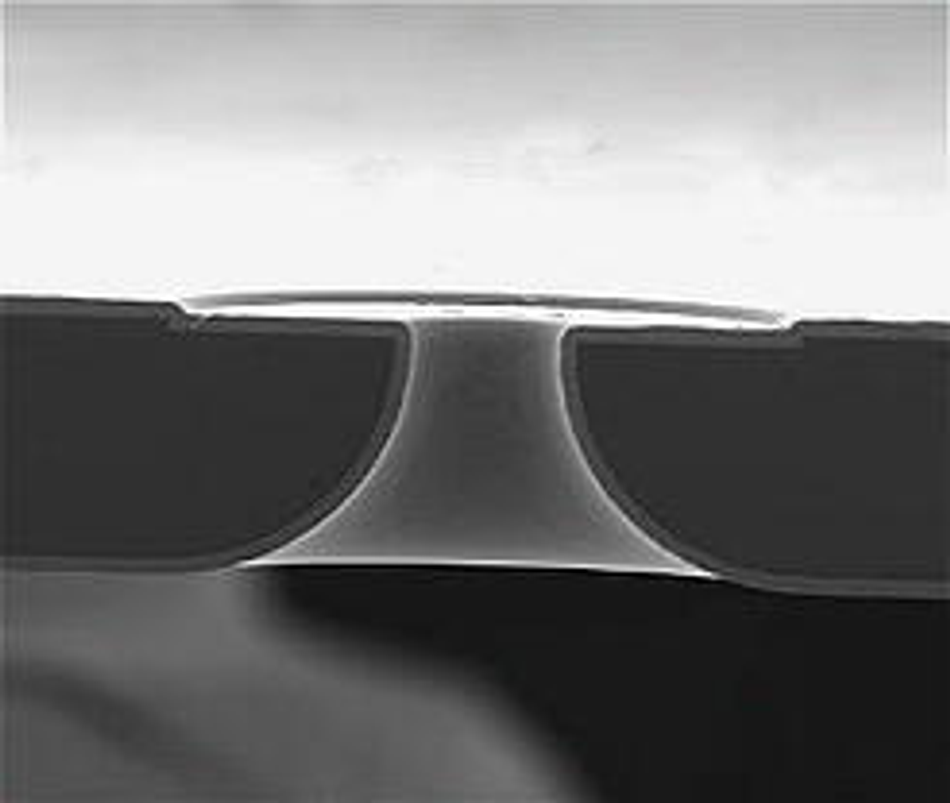
image 2. An electroformed, high-precision PV cell stencil, by Veco B.V.
(3) Inkjet printing
Inkjet printing is an extremely versatile, non-contact process that involves jetting tiny ink droplets to facilitate direct printing. Besides printing graphics on all kinds of surfaces, industrial inkjet printers today can deposit a wide range of inks with ultra-precise accuracy on various substrates. Thanks to inkjet printing being non-contact and that available inks range from polymers and metal nanoparticles to living cells, inkjet printing has seen a surge of new applications in fields including electronics, life science, optics, and PV.
In PV cell manufacturing, inkjet printing deposits metal paste directly onto the surface of the cell through very minuscule openings of a highly efficient, parallel print head, providing a contactless, maskless printing alternative to conventional screen printing and stencil printing. This dispensing process provides the PV industry with multifaceted benefits over conventional screen printing, such as those outlined below.
→ Increased efficiency and electricity output
In screen printing, a squeegee is used to push the metal paste through the screen openings and onto the wafer surface. The typical line width is 55–80 μm, resulting in a shadowing loss of 7–10 percent. Moreover, lines have a low aspect ratio of c.a. 0.2–0.5.
In inkjet printing, the lines can be made much thinner, exposing a larger semiconductor surface to the sunlight. The lines also have a better aspect ratio, ensuring a larger portion of incoming sunlight is reflected toward the wafer instead of back into the air. These two factors increase efficiency by approximately 1 percent and electricity output by.
→ Reduced metal paste consumption
In screen printing, the wire mesh and emulsion screens are repeatedly used and the openings can gradually get blocked or deform, resulting in lines broadening, becoming irregular, and having ragged edges.
In inkjet printing, finer lines with higher aspect ratios and lower striations can be achieved. Moreover, high-speed dispensing using the intermittent parallel operation of hundreds of nozzles down to several microns can be flexibly optimized in terms of nozzle number and arrangement. The accuracy and flexibility enable homogeneous line shape, contributing to a 20 percent reduction in metal paste consumption.
→ Significant throughput potential
Inkjet printing, being non-contact, promises a lower reject rate if used on thinner Si wafers. Also, being inline increases throughput significantly over conventional screen printing.
To sum up, the maskless nature of inkjet printing affords a high material utilization rate, improved output and efficiency, freedom of design, and significant throughput potential. Moreover, it can be directly integrated into an existing silicon PV cell production facility, replacing the screen printing process utilized for front-side metal contacts.
How electroforming has empowered the contactless metallization process
A vital part of the dispensing print head is the high-precision nozzle plate, produced using electroforming, a micro-precision, metal additive manufacturing (AM) process combining lithography and electrodeposition. The nozzle plate is a rectangular, elongated part with miniature holes, through which the metal paste is pressed and deposited via the nozzles onto the PV cell in very thin straight lines.
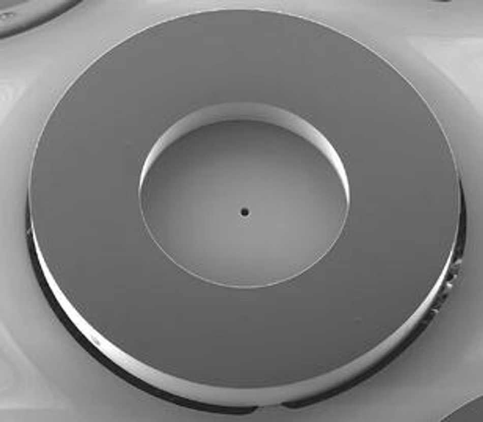
It is the complicated combination of accuracy, precision, material properties, and unique geometries enabled by electroforming that makes the plate an essential part of the dispensing print head. The miniature holes need to be down to several microns and perfectly round, true circles. Traditional cutting and drilling processes might not meet the stringent accuracy and precision requirements, and etching and laser processes could result in thermal stress and microburrs. Electroforming, on the other hand, does not influence metal properties such as hardness, grain structure, or ductility. It allows for the realization of high-precision products that are thermal stress- and microburst-free, providing absolute accuracy and high aspect ratios.
Another significant advantage of electroforming is reproducibility. The process affords a precision of approximately 5 μm. In a plate that has 100 to 200 miniature nozzles in a straight line, each of those nozzles needs to be the correct size, not only on each plate but on every plate and across different batches of the plate. Electroforming guarantees reproducibility, meaning the same drawing and process setup translates to perfectly uniform and reproducible printing results and the exact same product time and time again.
Electroforming can also be used to produce special hole geometries; for example, bell mouth shaped holes are not achievable using traditional cutting and drilling processes. These holes can effectively reduce blinding/clogging of the plate/nozzles, thus ensuring exceptional paste release performance.
A final point of note is that plate material resistance is especially important in PV cell production because the metal paste used can be corrosive. Also, the pressure applied to push the paste through the plate makes deformation a potential risk. For these reasons, Veco offers a range of alloys that have highly stable contact resistance and excellent mechanical characteristics, ensuring exceptional printing performance over a longer lifetime.