In new lab tests GaN-on-GaN transistors drop the slow trap component seen on SiC
Mitsubishi Electric measured transistor admittance from nanoseconds to milliseconds, aiming at simpler predistortion for base-station, radar and microwave heating amplifiers around 2030

16 Nov, 2026. 4 minutes read
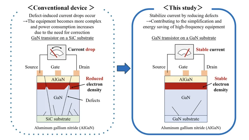
Comparison of crystal defects in GaN epitaxial layers on SiC and GaN substrates
What was announced
Mitsubishi Electric announced that gallium nitride (GaN) high-electron-mobility transistors (HEMTs) grown on free-standing GaN substrates show significantly less frequency dispersion than GaN HEMTs on silicon carbide (SiC), the usual substrate for GaN RF transistors. The company defines frequency dispersion as current and other characteristics varying with operating frequency, and attributes it to crystal defects formed when GaN is grown on SiC. Mitsubishi Electric says a new circuit analysis method including defect response let it link the two, and that the flatter response allows simpler digital correction circuits. [1]
Why it matters
Mitsubishi released a plot of the real part of the forward admittance, y21, for both substrates against the signal period, from nanoseconds to milliseconds. At these frequencies y21 reflects transconductance, and its dispersion is an established probe of deep-level traps, such as iron-related acceptors in the buffer and surface donor states, which often respond below 1 MHz. Read from the plot, both curves rise about 2% between 100 ns and 3 µs; the GaN-on-SiC curve then climbs roughly 5% more towards 10 ms, while the GaN-on-GaN curve stays flat.[1][3]
Over microseconds to milliseconds, trapping makes amplifier gain history-dependent. In a 500 W GaN-on-SiC Doherty base-station amplifier, University of Colorado and University of Bologna researchers measured trap-recovery time constants of about 100 µs and 2.1 ms, and memoryless digital predistortion (DPD) gave about 4 dB lower adjacent-channel leakage when signal peaks recurred faster than 100 µs. Doherty amplifiers usually need DPD anyway.[4] A transistor without the slow component would shrink the memory the predistorter has to model.
The substrate effect has precedents, including Mitsubishi Electric's own. At the 2024 CS MANTECH conference, the company reported 3.0×10⁶ cm⁻² etch-pit dislocations on GaN substrates, 1/230 of its GaN-on-SiC count, with less current collapse and lower two-tone intermodulation distortion at 2.4 GHz. Fujitsu reported similar dislocation and current-collapse gains in 2022, then 85.2% power-added efficiency at 2.45 GHz in 2025. The new measurement adds a timescale: only the response slower than a few microseconds differs between the substrates.[1][5][6][7]
The substrate is not the only trap source. With identical iron-doped buffers, the Berlin research institute Ferdinand-Braun-Institut (FBH) found comparable pulsed current collapse on both substrates, plus a silicon-contaminated substrate interface that cut 20 GHz power-added efficiency to 15% or less, against 46% to 50% on SiC.[8]
For base-station, radar and industrial microwave heating amplifier designers, this is a materials lever to track rather than a part to evaluate: Mitsubishi Electric targets deployment around 2030.[1]
Technical specifications: Mitsubishi Electric GaN-on-GaN versus GaN-on-SiC test transistors (IWN2026 result)
| Parameter | Value |
|---|---|
| Device | AlGaN/GaN transistor, as drawn in the company's illustration |
| Substrates compared | Free-standing GaN; SiC as reference |
| Measured quantity | Real part of admittance y21 versus signal period |
| Period axis of published plot | 10⁻⁹ s to 10⁻¹ s |
| Reported result | Frequency dispersion significantly suppressed on GaN substrate, with flat frequency characteristics (company description) |
| Analysis method | Circuit analysis incorporating defect-related response; model details not stated |
| Bias point, gate periphery, RF operating frequency | Not stated |
| Output power, efficiency, linearity | Not stated for these devices. The company's 2024 test transistors (1.0 µm gate): lower third-order intermodulation distortion and about 6 points higher PAE than GaN-on-SiC at 2.4 GHz |
| Dislocation densities | Not stated for these devices. The company's 2024 test transistors: 3.0×10⁶ cm⁻² on GaN by etch-pit count, 1/230 of its GaN-on-SiC count |
| Status | Research result; practical deployment targeted around 2030 |
| Programme | Japan Ministry of the Environment project; Mitsubishi Electric participating since 2024 |
| Presentation | IWN2026 talk JT1-3, 9 November 2026 |
Published GaN-on-GaN RF HEMT results for context (test conditions differ)
| Parameter | Fujitsu (2022) | Fujitsu (2025) | FBH (2025) |
|---|---|---|---|
| GaN substrate | Free-standing GaN; epitaxial dislocation density below 10⁶ cm⁻² (2×10⁸ cm⁻² on SiC) | 4-inch semi-insulating HVPE GaN, below 5×10⁶ cm⁻² | 2-inch semi-insulating Mn-doped GaN, 3×10⁷ to 6×10⁷ cm⁻² (about 5×10⁸ cm⁻² on SiC reference) |
| Gate length | 0.5 µm | 0.5 µm | 150 nm and 190 nm |
| Large-signal result | 64.3 W and 71.1% PAE at 2.6 GHz, pulsed (10 µs, 1% duty); 54.6 W and 63.3% PAE in CW | 85.2% PAE, 89.0% drain efficiency, 7.9 W/mm at 2.45 GHz and 55 V, pulsed (10 µs, 1% duty) | 1.3 to 1.7 W/mm and 10% to 15% PAE at 20 GHz and 20 V (SiC reference: 2.5 to 2.6 W/mm, 46% to 50%) |
| Pulsed current collapse | Lower than GaN-on-SiC | No significant change versus Fujitsu's earlier GaN-on-GaN devices | Comparable to or slightly lower than GaN-on-SiC |
| Thermal | Heat dissipation comparable to GaN-on-SiC after backside processing | Not reported | About 100 K/W versus 75 K/W on SiC (rough estimate) |
Sources: [1][2][5] (first table); [6][7][8] (second table)
Mitsubishi Electric's comparison is a small-signal measurement at an unstated bias. Trapping in GaN amplifiers is set largely by peak gate and drain voltages under RF drive,[4] so a design decision needs large-signal output power, efficiency and linearity under modulated signals. The company's 2024 test transistors showed lower two-tone distortion and about 6 points higher power-added efficiency on GaN at 2.4 GHz,[5] but neither that paper nor the announcement includes a modulated-signal or predistortion result.
The substrate also changes the thermal path: FBH estimated about 100 K/W on GaN against 75 K/W on SiC for its test transistors,[8] which weighs most in continuous-wave uses such as microwave heating.[6]
References
- Mitsubishi Electric Achieves World's First Demonstration of Suppression of Frequency Dispersion in GaN Transistors Using GaN Substrates (release No. 3953, PDF version), Mitsubishi Electric, 9 November 2026. Company press release; the PDF carries the Features section and the y21 plot that the web version omits.
- IWN2026 Advance Program (program only), International Workshop on Nitride Semiconductors 2026, 2026. Conference program; lists talk JT1-3 and other GaN-substrate papers.
- Identification of Buffer and Surface Traps in Fe-Doped AlGaN/GaN HEMTs Using Y21 Frequency Dispersion Properties, P. V. Raja et al., Electronics (MDPI), 13 December 2021. Peer-reviewed, open access.
- Linearization of a 500-W L-band GaN Doherty Power Amplifier by Dual-Pulse Trap Characterization, T. Cappello, C. Florian, A. Santarelli and Z. Popović, IEEE/MTT-S International Microwave Symposium, 2019. Author copy of a conference paper.
- X-band GaN HEMT and Free-standing GaN Substrate for Marine Radar, E. Yagyu et al., CS MANTECH, May 2024. Conference paper by Mitsubishi Electric and Furuno Electric.
- GaN RF HEMTs: Powering ahead with native substrates, N. Okamoto and Y. Kumazaki, Compound Semiconductor, 1 February 2022. Magazine feature written by the Fujitsu researchers.
- AlGaN/GaN HEMT on a free-standing GaN substrate with record 85.2% power-added efficiency at 2.45 GHz, T. Ohki et al., Applied Physics Express, 19 March 2025. Peer-reviewed, open access.
- Impact of Parasitic Conductive Interfaces on the DC and RF Performance of GaN-on-GaN HEMTs, A. Bassal et al., physica status solidi (a), 8 September 2025. Peer-reviewed, open access.