Cutting Chemicals, Cutting Carbon: How Dry Phase Patterning Is Greening Flex-PCB Manufacturing
Discover how Dry Phase Patterning (DPP) showcased a 99 percent reduction both in carbon footprint and electricity used compared to conventional wet etching.

18 Jun, 2025. 6 minutes read
Today, wet etching is among the most common methods used in the manufacturing of electronic chips. Yet while reliable at making circuits on a mass scale, this approach has a big problem associated with it: its environmental cost, particularly when it comes to water consumption and contamination. With limited freshwater resources—and as many as three billion people worldwide experiencing regular water shortages[1]—the electronics industry must urgently turn to new solutions that are less reliant on H2O and more sustainable overall. Swedish company DP Patterning has developed one such solution, Dry Phase Patterning (DPP), a patented continuous FPCB production technique that not only reduces wastewater dramatically, but also cuts carbon footprint by 99% and simplifies production workflows.
As we’ll see in more detail in this article, DPP offers an alternative to other FPCB production techniques. Compared to wet etching, the technology has a number of sustainable benefits, which are illustrated in the table below:
Dry Phase Patterning (DPP) | Wet Etching |
Uses single material (laminate) | Requires multiple materials |
Low power consumption | High power consumption |
Does not use any corrosive chemical | Requires dangerous corrosive chemicals |
No reliance on freshwater | Heavy reliance on freshwater and water cleaning treatments |
Material waste is 100% recyclable | Waste typically ends up in landfill |
Safe for operators | Operators must take precautions working with corrosive chemicals |
Dry Phase Patterning, a sustainable alternative
In order to achieve net zero by 2050 (as stated in the Paris Agreement), industries around the world must reduce emissions by 45% (from 2010 levels) within the next five years. The electronics industry, which generates emissions in a number of ways, therefore must find solutions to improve its eco-footprint.
DP Patterning’s patented Dry Phase Patterning (DPP) process offers a strong alternative to conventional production techniques like chemical wet etching, providing benefits of cost reduction and sustainable production. DPP is a mechanical process that can create flexible circuit boards in a safe, continuous, and highly efficient manner.
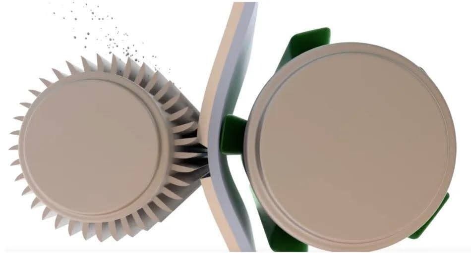
The technology consists of a few simple steps: first, a cliché tool presses a pattern onto a laminate material (itself comprising a top layer and substrate). This laminate (typically using a metal such as aluminum or copper clad aluminum) is installed on a roll-to-roll system, enabling continuous processing at a rate of up to 30 meters per minute. A precision milling wheel with a resolution of 250 nm then removes the cliché pattern from the top layer of the laminate, resulting in a conductive pattern on the substrate.
Moreover, the DPP solution developed by DP Patterning is all in one, meaning that it integrates the entire production chain into a single system, including the magnetic roll-to-roll setup for the laminate material and an easy-to-swap tooling system to enable rapid pattern changes. According to DP Patterning, this comprehensive solution for manufacturing flexible PCBs can unlock up to 10 times faster production rates.
The ecological benefits of DPP
DP Patterning’s patented DPP technology is far more sustainable than conventional FPCB production techniques in virtually all ways. As we’ll see in more detail, the innovative process addresses many of the ecological issues associated with wet chemical etching.
No chemicals required
One of the key sustainable benefits associated with DPP technology is related to the simple fact that it is an entirely mechanical process. This means that it does not require the use of any chemicals, making it far less environmentally costly than chemical etching techniques and far safer to operate.
Wet chemical etching, by contrast, is a process that uses liquid chemicals (aka etchants) to dissolve material from a substrate in a specific pattern. Etchants used in the process, such as hydrochloric acid, nitric acid, ferric chloride, or potassium hydroxide, along with particles of the substrate removed in the wet etching process, contaminate water, resulting in significant volumes of wastewater tainted by heavy metals and corrosive solvents. This wastewater, which can be both cytotoxic and genotoxic[2], must therefore undergo treatments, which can themselves be energy intensive and require the use of more chemicals.
Reduced water consumption
One of the main ecological problems faced by electronics manufacturers is the consumption of freshwater, specifically ultrapure water, which undergoes treatments like deionization and reverse osmosis to be suitable for circuit board processing. According to the World Economic Forum, the average chip manufacturing facility can consume 10 million gallons of ultrapure water every day.[3] In the case of FPCB production using wet chemical etching, ultrapure water is used primarily in the cleaning process to rinse away etchants from the circuit.
The DPP workflow, for its part, does not necessitate the direct consumption of water, reducing the reliance on freshwater resources in the production of flexible electronics. Overall, DP Patterning’s solution not only doesn’t produce toxic wastewater, it doesn’t require water to operate (manufacturers can optionally use water in a cleaning step).
Recyclable scrap
Another key ecological advantage offered by DPP technology is related to the reduction in waste material. Whereas wet chemical etching generates significant waste (including all the chemicals and heavy metals removed through water treatments), the only leftover material generated in the DPP process is clean metal flakes. The aluminum flakes, effectively what is cut away from the laminate, can be recycled in full.
Less energy intensive
The mechanical FPCB processing method also eliminates any energy consumption resulting from post-curing, since the flexible circuits do not involve any ink-based materials that require heat-based curing. Instead, the mechanical patterning process results in conductive FPCBs that require very little post-processing.
Simple supply chains
Since DPP uses far fewer consumables (essentially just the laminate and small amounts of lubricant), supply chains are far simpler than other circuitry workflows. This not only has an impact by way of minimizing carbon emissions associated with complex logistics and transport networks, but also on the manufacturer’s bottom line.
Dry Phase Patterning LCA
While the sustainable benefits of DPP can be understood by simply looking at how the process works, there is also impressive data to back it up. In a life-cycle analysis (LCA) carried out by the Fraunhofer Institute comparing DPP and conventional wet etching, the DPP process showcased a 99% reduction both in carbon footprint and electricity used.
Manufacturing method | Carbon footprint (kg CO₂ eq) | Electricity used |
Dry Phase Patterning (DPP) | 0,15 | 0,2 kWh |
Conventional wet etching | 18,8 | 19 kWh |
Percentage sustainability benefit | 99% reduction | 99% reduction |
In this LCA, the Fraunhofer Institute used a functional unit (FU) of 35 µm copper on a 50 µm PET carrier for wet etching and a 18 µm aluminium conductive layer on the same 50 µm PET carrier (the discrepancy in the FU is based on the material efficiency of the DPP process). As DP Patterning explains: “A material choice can be based on prices and old habits, not on material efficiency, therefore having more material than needed for the conductive constraint.”
Test your global impact! The DP Patterning’s Global Impact Calculator can reduce the global footprint from your production by replacing hazardous chemical etching processes by sub-suppliers with an in-house, mechanical reel-to-reel process. Follow the link to test your global impact with their process! |
Towards a new sustainability standard with DPP
DP Patterning’s sustainable solution is already being embraced by innovative industrial players. Dry Phase Patterning production is used for applications ranging from different types of antennas, heaters, FPC for LED lighting and CCS (Cell Connecting Systems) used in (EVs) and hybrid electric vehicles (HEVs).
Ultimately, all industries that use flexible printed circuit boards can benefit from Dry Phase Patterning, particularly if they are invested in pursuing a more sustainable future for electronics. Electronics manufacturing, currently so closely associated with water depletion, pollution, and energy intensive processes, could be radically transformed by solutions like DPP, which take an outside-of-the-box, environment-first approach without compromising on productivity.
If you are facing challenges greening internal or outsourced FPCB production, the DP Patterning team would love to hear your perspective and to share how DPP could be transformative. Connect with DP Patterning via email or continue the conversation on LinkedIn.
Resources
[1] Imminent risk of a global water crisis, warns the UN World Water Development Report 2023 [Internet]. UNESCO, March 22, 2023. https://www.unesco.org/en/articles/imminent-risk-global-water-crisis-warns-un-world-water-development-report-2023
[2] Gerić M, Gajski G, Oreščanin V, Domijan AM, Kollar R, Garaj-Vrhovac V. Environmental risk assessment of wastewaters from printed circuit board production: A multibiomarker approach using human cells. Chemosphere. 2017 Feb 1;168:1075-81. https://doi.org/10.1016/j.chemosphere.2016.10.101
[3] James, Kirsten. The water challenge for semiconductor manufacturing: What needs to be done? [Internet]. World Economic Forum, July 19, 2024. https://www.weforum.org/stories/2024/07/the-water-challenge-for-semiconductor-manufacturing-and-big-tech-what-needs-to-be-done/
[4] 8 Things You Should Know About Water & Semiconductors [Internet]. CWR, July 11, 2013. https://cwrrr.org/resources/analysis-reviews/8-things-you-should-know-about-water-and-semiconductors/
[5] Our partners for Electronica 2024 [Internet]. DP Patterning, October 29, 2024. https://dppatterning.com/our-partners-for-electronica-2024/