An introduction to Integrated Photonics
Article 1 of our Integrated Photonic Series: Integrated Photonics is set to revolutionize electronic devices, circuits, and telecommunication systems

Last updated on 17 Nov, 2020. 6 minutes read
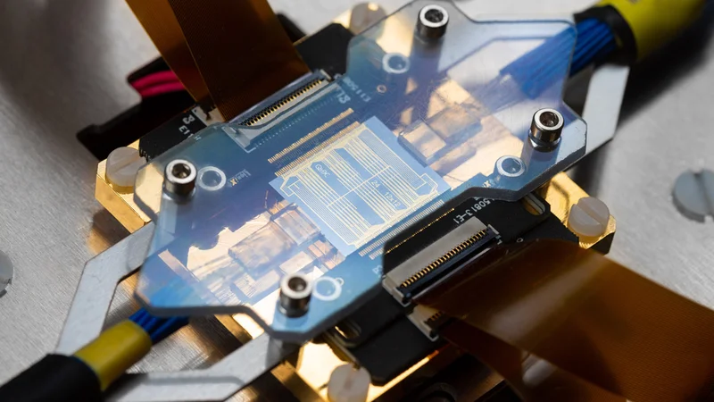
PHIX – Gijs van Ouwerkerk, courtesy of QuiX
This is the first article in a series dedicated to integrated photonics. In this article, we introduce you to the technology, its history, and its materiality.
What is integrated photonics?
Integrated Photonics (IP) is the use of light for applications traditionally tackled by electronics. It can be used in a wide range of areas including telecommunications such as 5G networks, biosensors for speeding up medical diagnosis, and in automotive where it is used in LiDAR. IP consists of integrating multiple photonic functions on a Photonic Integrated Circuit (PIC) fabricated using automated wafer-scale generic integration technology over silicon, silica, or Indium Phosphide (InP) substrates. Integrated photonics dramatically improves the performance and reliability of these photonic functions while simultaneously reducing the size, weight, and power consumption.
Electronics versus Photonics
A good introduction to IP is by understanding its similarities and differences with traditional electronic circuits. Where electronics deal with the control of electrons on a chip, photonics does the same with photons. Photons are the fundamental particles of light.
Conventional integrated circuits (ICs) conduct electricity by allowing the flow of electrons through the circuit. Electrons are negatively charged subatomic particles that interact with both other electrons and other particles. These interactions slow electrons down as they move through circuits, this limits the amount of information that can be transmitted; it also generates heat, which in turn causes energy and information losses.
Photonic integrated circuits (PICs) use photons. Photons move at the speed of light with almost no interference from other photons. This greatly increases the bandwidth (the data transfer rate) and speed of the circuit, without big energy losses making PICs significantly more efficient than their IC counterparts.
Integrated photonic components use "waveguides", which confine and direct the light in the desired directions (by total internal reflection), much the same way as metallic wires do for electrical signals. A PIC provides functions for information signals on optical wavelengths typically in the visible spectrum or near-infrared 850 nm-1650 nm.
The elements on a PIC are connected via waveguides. The chip elements can be both passive (e.g. couplers, switches, modulators, multiplexers) and active (e,g amplifiers, detectors, and lasers). These components are integrated and fabricated onto a single substrate, which creates the compact and robust photonic device.
A key difference between electronic circuits and PICs is in the primary device that is used for fabrication. In an electronic integrated circuit, the main device is the transistor. But, in PIC, there is no particular main device that dominates in the fabrication. According to its application, the PIC will be designed with a range of fabrication devices. This integration presents opportunities to reduce current bulky, complex, and expensive optical systems in an integrated chip-scale way that has increased stability and robust operation, reduced size and power consumption, and cost-effective large-scale fabrication of even complex circuits.
Fabrication and materials
PICs are currently fabricated on both standard element semiconductors and compound semiconductors to dielectric materials and nonlinear crystal materials. The specific application requirements drive the choice of the most suitable substrate material as each material has its own specific advantageous features and limitations. For example, lithium niobate can be used to fabricate low-loss waveguide devices or integrated flexible chalcogenide glass to make photonic crystals with mechanical flexibility.
The transparency and refractive index of the materials as well as their ability to directly generate light defines the properties of the finished PIC and its uses. The material's bend loss and bend radius also impact the PIC properties. Bend loss describes propagation losses (reduction in power density) in an optical fiber (or other waveguide) caused by bending while the bend radius describes the amount a fiber can bend without breaking. The major substrates today are Indium Phosphide (InP)-based monolithic integration and Silicon Photonics but Silica (SiO2 and Silicon Nitride (SiN) are also growing areas.
Indium Phosphide (InP)
Indium phosphide (InP) is the most developed platform for PICs. InP allows for the integration of both active and passive elements such as high-performance amplifiers, lasers, modulators, and detectors in combination with interferometers within one chip in the 1.1 – 1.6 μm spectral window. InP integrated photonics are used in data communications, precision metrology (for example LIDAR in autonomous vehicles), spectrometry, and imaging.
Much of the most impactful research into InP has been done in the Netherlands and several organizations and research groups continue to lead the way. The Smart Photonics foundry in Eindhoven is a leader in production services for Indium Phosphide based photonic components. The foundry and its associated services offer support for researchers and businesses to test and expand their use of InP PICs.
Silicon Photonics (SiPh)
Building on the success of silicon (Si) as the foundation of IC reliability, silicon photonics (SiPh) is a critical part of integrated photonics development. Silicon photonic devices can be manufactured using existing semiconductor fabrication techniques, and as silicon is already used as the substrate for most ICs, both optical and electronic components can be integrated on to the chip to create hybrid devices.
Si is transparent to infrared light with wavelengths above about 1.1 micrometers (μm) - making it suitable for fiber optic telecommunication systems which uses 1.55 micrometer wavelength. It also has a very high refractive index, of about 3.5, much higher than that of silicon oxide (1.5), which allows strong confinement of light in Si structures embedded in silicon oxide (waveguides). These properties make Si well suited for usage in telecom.
Silicon Nitride (SiN)
Silicon Nitride (SiN) based platforms are of recent growing interest due to their large transparency window (from visible to MIR) and ultra-low optical losses compared to other PIC platforms. Silicon nitride (SiN) excels at passive light processing in the visible, near-infrared (NIR), and IR range thanks to its very low light intensity loss in the waveguide, small bend radii, and adjustable polarization. If required by the application, active components made in another technology platform (i.e. InP) can be coupled to SiN PICs into the same package through PIC-level hybrid integration processes.
The proprietary waveguide concept, called TriPleX, from the Dutch company, Lionix International, has the lowest propagation losses reported for silicon nitride waveguides (0.1 dB/cm down to 0.1 dB/m). It operates in a broad wavelength band ranging from 405 nm to 2350 nm. Furthermore, they have developed a patented tapering method that converts low contrast modes for optimal fiber coupling, to high contrast modes for small bending radii.
There are several large scale research projects underway that are aiming to eliminate the number of current assembly steps and provide both lossless transitions between materials and a lower-cost manufacturable process.
Lithium niobate (LiNbO3)
Lithium niobate (LiNbO3) is a nonlinear crystal material suitable for devices performing nonlinear functions - that is functions that take advantage of this material property. A good example electro-optic modulators or acousto-optic transducers. Waveguides can be fabricated on lithium niobate substrates controlled by a lithographic method. Adding or ‘doping’ rare-earth ions to Lithium niobate makes amplifiers and lasers possible. LiNbO3 has the property of birefringence - which means its refractive index depends on its polarization direction. This creates opportunities for polarization control, which may then be used for filtering purposes or other similar applications. However, this property also makes it more difficult to form polarization-independent devices, which are often required for optical fiber communications.
Innovation through collaboration
PhotonDelta, a Dutch public-private partnership consisting of a cohesive cluster of companies and highly qualified knowledge institutes, has been formed to accelerate and reduce time to market of integrated photonics products. PhotonDelta stimulates and facilitates cooperation between stakeholders within the ecosystem providing fertile ground for developing the common business strategy, setting goals, and stimulating cooperation between partners in the Netherlands and beyond. PhotonDelta helps to amplify and scale existing companies and kickstart new ones by having access to significant funding through its industry building and growth accelerator program.
Conclusion
Integrated Photonics is an emerging field of technology already demonstrating massive future potential in applications across multiple fields. Much of this emerging industry developments/scale-ups and relevant R&D are occurring in the Netherlands supported and driven by the leadership of PhotonDelta. PICs will continue to increase in efficiency and speed, both driving disruptive innovation, I.e. enabling (radically) new products and markers, as well as improving existing systems.
In our next article, we explore the key technology areas for Integrated Photonics. We’ll guide you through how the technology is impacting automotive, biosensors, communications, quantum computing, and data storage.
About the sponsor: PhotonDelta
PhotonDelta is a growth accelerator for the Dutch integrated photonics industry. Its objective is to promote the adoption of integrated photonics and support companies to get prioritized access to the Dutch Integrated Photonics supply chain. Furthermore, PhotonDelta runs a new business creation program that provides companies, ranging from startups to SMEs and big organizations, with access to strategy, market, and funds.
Through its wide network within the industry, PhotonDelta has gathered insights on market trends, challenges, and product roadmaps. This information is used to drive business creation, investments, and strategic technology roadmaps. Furthermore, PhotonDelta actively supports start-ups and SMEs to facilitate their involvement with the Dutch integrated photonic supply chain. This includes facilitating options for establishing a solid presence in the Netherlands.