Secure-control FPGA puts post-quantum root of trust on 215k-logic-cell device
Lattice's Mach-N2 FPGAs pair internal-flash boot with PCIe Gen4 and 16 Gb/s transceivers for compute and communications infrastructure.

30 Sep, 2026. 5 minutes read
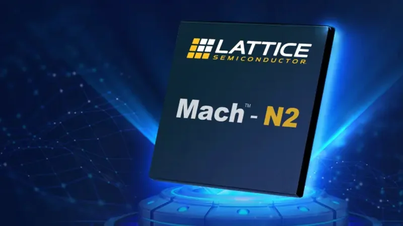
The Lattice Mach N2 FPGA
Lattice Semiconductor announced the Mach-N2 Family:
The Mach-N2 is the newest generation of Lattice's secure-control FPGAs, which handle power sequencing, system management and security. Mach-N2 shares Nexus 2, Lattice's 16 nm FinFET platform, with the general-purpose Certus-N2 family, adding internal flash and run-time security. Its five devices span 40k to 135k LUTs, or 65k to 220k system logic cells.[1][2][3]
Lattice says Mach-N2 pairs a hardware root of trust with crypto-agile post-quantum cryptography (PQC) compliant with CNSA 2.0, the NSA's algorithm suite for national security systems. It also claims up to twice the logic density for system control functions and sub-30 ms boot for the 220k-cell device.[1] Hardware PQC sits on one device, the 215k-cell MH21D.[2]
Why it matters
Lattice pitches Mach-N2 as a first-on, last-off device.[4] In NIST's platform firmware resiliency model, SP 800-193, a root of trust protects firmware, detects corruption and restores a known-good image.[5] The NSA prioritises firmware signing, whose algorithms are "frequently locked in for the life of a system". CNSA 2.0 lists hash-based LMS and XMSS for firmware signing, ML-DSA-87 for signatures and ML-KEM-1024 for key establishment, and new national security system acquisitions must comply from January 1, 2027.[6]
The MH21D adds ML-DSA, LMS, XMSS and stateless hash-based SLH-DSA signatures, plus ML-KEM key exchange, to the classical cryptography all five devices share.[2] Lattice's previous PQC-capable parts belong to its MachXO5-NX secure-control family, whose TDQ devices launched in October 2025 on 28 nm FD-SOI and now reach 64k logic cells with PCIe Gen2 x1.[7][8] The MH21D's 132k LUTs are about 2.5 times the largest TDQ device's roughly 53k (author's calculation, 64k cells ÷ 1.2 cells per LUT), and its hard PCIe controller runs Gen4 x4.[2]
The MH21D comes only in an 18 × 18 mm CBG484 package with 236 user I/O and in the two slower speed grades; it needs customer keys and policy provisioned before first use. Mach-N2 tops out at 248 user I/O, 92 of them 3.3 V-capable, where the largest MachXO5-NX packages reach 360 or more, over 300 of them 3.3 V-capable. Mach-N2 also drops the 12-bit SAR ADCs that MachXO5-NX provides for system monitoring.[2][8][9]
Some competing FPGAs already offer post-quantum boot. AMD's cost-optimised Spartan UltraScale+ SU200P targets board management and platform root of trust with up to 572 I/O and up to eight transceivers. The SU200P authenticates boot images with hash-based HSS/LMS signatures or ECDSA P-384 and receives its configuration from external memory or a host at every power-up.[10][11][12] Altera said in September that PQC-enabled Agilex 3 and Agilex 5 FPGAs are shipping.[13] Mach-N2 instead boots from internal flash; Lattice says configuration data is never exposed outside the device while loading.[14]
Technical specifications
Mach-N2 devices
| Spec | MH06 | MH10 | MH16 | MH20 | MH21D |
|---|---|---|---|---|---|
| System logic cells | 65k | 100k | 160k | 220k | 215k |
| LUTs | 40k | 61k | 98k | 135k | 132k |
| Block RAM (36 kbit blocks) | 114 | 153 | 228 | 306 | 289 |
| 18 × 18 multipliers | 120 | 240 | 360 | 520 | 520 |
| Hardware PQC and crypto agility | No | No | No | No | Yes |
| Packages (0.8 mm pitch) | CBG256 (14 × 14 mm), CBG484 (18 × 18 mm) | CBG256, CBG484 | CBG484 | CBG484 | CBG484 |
| User I/O, total (3.3 V-capable wide-range / high-performance) | 141 (39 / 102) in CBG256; 196 (92 / 104) in CBG484 | 141 (39 / 102) in CBG256; 196 (92 / 104) in CBG484 | 248 (92 / 156) | 248 (92 / 156) | 236 (83 / 153) |
| Transceiver lanes | 2 in CBG256; 4 in CBG484 | 2 in CBG256; 4 in CBG484 | 4 | 4 | 4 |
| Speed grades | 1 to 3 | 1 to 3 | 1 to 3 | 1 to 3 | 1 and 2 |
| User flash memory (UFM) | not stated | not stated | 105,472 kbit | 105,472 kbit | not stated |
| Internal flash, total | not stated | not stated | not stated | 256 Mbit | not stated |
| Configuration time | not stated | not stated | not stated | under 30 ms (Lattice claim) | not stated |
| Flash data retention at 100 °C junction | 20 years | 20 years | 20 years | 20 years | not stated |
| Flash programming cycles within retention spec (write/erase maximum) | 10,000 (100,000) | 10,000 (100,000) | 10,000 (100,000) | 10,000 (100,000) | not stated |
Shared by all five Mach-N2 devices
| Spec | Value |
|---|---|
| Platform and process | Lattice Nexus 2, TSMC 16 nm FinFET |
| Core supply | 0.82 V |
| Transceivers | up to 16 Gb/s per lane |
| PCIe | hard Gen4 (16 GT/s) controller, up to x4, up to eight physical functions |
| Ethernet | 10GbE, with PMA and PCS in hardware and the MAC in fabric |
| External memory | DDR4 and LPDDR4 up to 2400 Mb/s |
| Configuration | boots from internal flash (self-download mode); images programmed over JTAG or target SPI; no boot from external SPI flash |
| Image fallback | up to three stored images: primary, secondary and golden (Lattice); falls back on a failed authentication or a bitstream revision below the set minimum |
| Bitstream protection | AES-256-GCM encryption; ECDSA (up to 521-bit) or RSA (up to 4096-bit) authentication |
| Run-time cryptography | AES-256 engines at up to 2.5 Gb/s and 10 Gb/s; SHA-2, SHA-3 and HMAC up to 512 bits; ECDSA, ECDH and ECIES up to 521 bits; Ed25519; RSA 2048 to 4096; TRNG |
| Device identity | physically unclonable function (PUF), 256 bits of entropy, stable for more than 20 years; Lattice lists DICE and SPDM attestation on the PUF-derived identity |
| Anti-tamper | voltage and temperature monitor, plus user-triggered responses ranging from zeroising RAM and stored secrets to permanently disabling the device |
| Temperature grades | commercial 0 to 85 °C; industrial -40 to 100 °C |
| Power consumption | not stated |
MH21D root-of-trust device: differences from the other four
| Spec | Value |
|---|---|
| Post-quantum signatures | ML-DSA, LMS, XMSS, SLH-DSA |
| Post-quantum key exchange | ML-KEM |
| Other additions | Ed448; SHAKE128 and SHAKE256; crypto agility with field-updatable algorithms (Lattice) |
| ML-DSA and ML-KEM parameter sets | not stated (CNSA 2.0 requires ML-DSA-87 and ML-KEM-1024) |
| Secret storage | one-time-programmable memory; the battery-backed RAM option is not available |
| Provisioning | customer policy and key files plus an authenticated image, loaded over JTAG or target SPI before the first reboot |
Sources: [1][2][3][4][14][15][16]
All Mach-N2 specifications are preliminary. Cell counts do not compare across generations: Nexus 2 system logic cells run about 1.63 per LUT against 1.2 for MachXO5-NX logic cells, so the 220k-cell MH20 has about 1.7 times the LUTs of the largest MachXO5-NX (our calculation).[2][9] Lattice quotes a boot time under 30 ms for the MH20, whose uncompressed bitstreams are 44 Mbit to 64.1 Mbit.[1][14] For CNSA 2.0 designs, the MH21D's parameter sets are a gating item; boot time and power only set budgets. Lattice's evaluation board carries an MH20, which lacks the PQC engines.[17]
Recommended reading: Post-quantum secure boot reaches low-cost and mid-range FPGAs. How Altera placed PQC bitstream authentication in the Agilex 3 and Agilex 5 Secure Device Manager, and where other vendors put it in the boot chain.
References
- Lattice Expands Secure Control FPGA Leadership with New Lattice Mach-N2 Family, Lattice Semiconductor via Business Wire, September 16, 2026.
- Lattice Nexus 2 Platform: Overview Data Sheet (FPGA-DS-02122, v0.80), Lattice Semiconductor, September 2026. Preliminary vendor datasheet.
- Lattice Advances Low Power FPGA Leadership with New Small and Mid-range FPGA Offerings, Lattice Semiconductor via Business Wire, December 10, 2024.
- Mach-N2, Lattice Semiconductor product page, accessed September 30, 2026.
- Platform Firmware Resiliency Guidelines (NIST SP 800-193), National Institute of Standards and Technology, May 2018.
- The Commercial National Security Algorithm Suite 2.0 and Quantum Computing FAQ, National Security Agency, December 2024. Cybersecurity Information Sheet, version 2.1.
- Lattice Launches Industry-First PQC-Ready FPGA Family: MachXO5-NX TDQ, Lattice Semiconductor via Business Wire, October 13, 2025.
- MachXO5-NX Family Root-of-Trust Devices Data Sheet (FPGA-DS-02120, v1.5), Lattice Semiconductor, August 2026. Vendor datasheet.
- MachXO5-NX Family Data Sheet (FPGA-DS-02102, v2.3), Lattice Semiconductor, July 2026. Vendor datasheet.
- AMD Spartan FPGA Grows Up: Bigger, Smarter, Scalable, More Secure, AMD, June 15, 2026. Vendor blog.
- Spartan UltraScale+ Authentication Certificate (Bootgen User Guide, UG1283), AMD, June 2026. Vendor user guide.
- Configuration Flow for AMD Spartan UltraScale+ Devices, AMD, 2025. Vendor presentation.
- Altera Adds Post-Quantum Security to Agilex 3 and Agilex 5 FPGAs, Altera press release, September 8, 2026.
- Lattice Nexus 2 sysCONFIG User Guide (FPGA-TN-02370, v0.82), Lattice Semiconductor, September 2026. Preliminary vendor technical note.
- Lattice Nexus 2 Platform: Specifications Data Sheet (FPGA-DS-02121, v0.80), Lattice Semiconductor, September 2026. Preliminary vendor datasheet.
- Lattice Nexus 2 Multi-Boot User Guide (FPGA-TN-02385, v0.81), Lattice Semiconductor, September 2026. Preliminary vendor technical note.
- Mach-N2 Evaluation Board (FPGA-EB-02078, v0.81), Lattice Semiconductor, September 2026. Vendor board guide.