Integrated Photonics Spotlight: Innovations in Sensing and Environmental Monitoring
Photonic integrated circuits are enabling smarter, faster, and more sustainable environmental monitoring.

25 Jun, 2025. 5 minutes read
When disaster strikes slowly, we often fail to see it coming. The air doesn't turn deadly overnight. Crops don’t fail in a day. But without precise, real-time environmental sensing, we miss the tipping points until it's too late.
With climate extremes intensifying and the world edging closer to the projected 250,000 annual heat-related deaths from 2030 to 2050, as predicted by the World Health Organisation (WHO), the urgency for more innovative environmental solutions has never been clearer.
Traditional sensors play a crucial role in addressing these dangers, including climate change, pollution, and food security. They assess air quality, manage water resources, and enhance crop yields. But the need for data that is faster, more precise, and more widely available is pushing existing sensors to their limitations.
This is where integrated photonics offers a transformative advantage. By uniting optical science with advanced microfabrication, Photonic Integrated Circuits (PICs) enable compact, resilient sensor architectures that leverage light for signal generation, transmission, and detection. These photonic chips deliver high-speed, high-precision environmental measurements with minimal power consumption. Their innate immunity to electromagnetic interference and suitability for harsh or remote deployments make them foundational to the next generation of intelligent, distributed sensing systems.
PhotonDelta initiated the Global Photonics Engineering Contest to explore the potential applications of this technology. The contest brought together engineers and academics from around the world to showcase new concepts that utilized PICs. One entrant that stood out illustrated how these chips might truly help sustainable farming by providing farmers on the front lines of climate change with more innovative tools.
The Changing Landscape of Environmental Monitoring: Why Demand Is Growing
Climate biodiversity variability, urbanization, loss, and rising populations are pushing governments and industries to monitor more, detect faster, and act smarter.
Applications of environmental sensing include:
Climate change monitoring (e.g., CO₂, methane, ocean acidification)
Air and water quality control
Precision agriculture and soil health
Industrial safety and emissions tracking
Biodiversity and ecosystem surveillance
To function effectively, these apps require monitoring systems that are accurate, real-time, and remote. However, making typical sensing systems larger to meet these needs can be challenging due to issues with power consumption, size, data transfer, and durability.
Limitations of Traditional Sensors
Conventional sensors, particularly those relying on electrical or mechanical mechanisms, face significant limitations in modern environmental monitoring. Their size and fragility make them unsuitable for deployment in harsh or remote field conditions. Sensitivity is often inadequate for detecting subtle chemical or biological changes, and high power consumption renders them impractical for off-grid or energy-constrained applications.
Moreover, many traditional systems struggle to support multiplexed sensing, limiting their ability to measure multiple parameters simultaneously. Finally, constraints in latency and bandwidth hinder their effectiveness in real-time data acquisition and transmission.
These limitations spotlight a growing need to transition away from legacy technologies toward next-generation sensing systems that are not only precise but also scalable, intelligent, and robust.
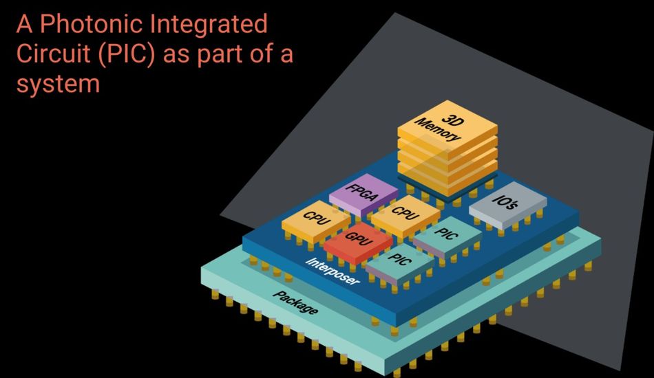
What Is Integrated Photonics?
PICs are microchips that combine multiple optical functions to create an optical circuit. These chips can generate, manipulate, and detect light. There has been a growing interest in research and commercial applications for PICs for various markets, including environmental sensing, as they offer compact optical solutions at a low cost when mass-produced.
Their key advantages include:
Miniaturization: Hundreds of photonic elements on a chip smaller than a coin
Multiparameter sensing: Capable of measuring chemical, physical, and biological parameters simultaneously
Immunity to electromagnetic interference, which affects many traditional sensors
Energy efficiency: Passive optical components can operate with minimal power
High-speed data capture and transmission, often compatible with fiber or wireless IoT systems
Applications are already expanding into gas sensing, LiDAR, optical biosensors, lab-on-chip diagnostics, and environmental surveillance, all of which are supported by real-time analysis and edge computing.
Designed for the Edge
One of the most compelling benefits of PIC-based sensors is their seamless compatibility with the Internet of Things (IoT) and edge computing platforms. As devices shrink and networks expand, sensors must not only collect data but also process and transmit it instantly, often without human intervention.
Photonic chips are uniquely suited for this challenge. They enable:
On-chip spectral filtering and signal processing
Integration with machine learning models for rapid inference
Wireless communication modules (e.g. LoRa, Wi-Fi)
Deployment in distributed, mesh-based sensor networks
As the integrated photonics industry matures, we’re seeing a convergence of optics, AI, and wireless infrastructure, a powerful combination for global-scale sensing.
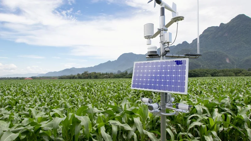
Global Engineering Entry Spotlight: Integrated Photonic Smart Soil Analyser (IPSA)
The Integrated Photonic Smart Soil Analyser (IPSA) is one of the best entries in the Global Photonics Engineering Contest. Engineer Jatinkumar Parmar and his team created this concept. The IPSA is a compact, high-precision device. It is designed to support real-time, on-site soil analysis for farmers, agronomists, and academics.
“Our goal with IPSA is to give farmers a smarter, more sustainable way to manage soil health, optimize yields, and conserve resources without needing a lab,” Parmar explains.
A silicon-based photonic integrated circuit makes up the central element of the IPSA. This circuit can detect a wide range of NIR and MIR wavelengths. These wavelengths can disclose soil pH, content, and more.
How It Works
IPSA integrates the following subsystems:
Multi-wavelength sensing array: using VCSELs and integrated waveguides to emit and capture reflected light signatures from soil samples.
On-chip spectral filters: isolating specific bands for targeted analysis of nutrients like nitrogen, phosphorus, and potassium.
Photonic signal processing: converting light signals to data using hybrid electronic-photonic processors.
Machine learning algorithms: predicting soil properties based on spectral data patterns.
Wireless communication module: transmitting data to a cloud dashboard via Wi-Fi or LoRa.
Mobile/web user interface: for visualizing soil health, trends, and real-time alerts.
Moving over big agricultural fields without disturbing the soil is easy with its handy design. Solar-powered and energy-efficient, the technology is ideal for resource-constrained places.
Why IPSA Matters
IPSA responds directly to the needs of modern precision agriculture. It enables:
Precision fertilization: reducing waste and runoff
Smart irrigation scheduling: based on real-time moisture data
Soil health tracking: monitoring organic matter, microbial activity, and pH over time
Contamination alerts: detecting heavy metals or high salinity levels
Sustainable crop planning: supporting crop rotation and soil regeneration efforts
From a technical standpoint, the project demonstrates what is possible when PICs, data science, and IoT are combined with in-depth domain knowledge in the agricultural sector.
IPSA is currently in the testing and validation phase, with field trials being conducted across diverse soil conditions. The team plans to move into pilot deployment and eventually scale up for commercial distribution.
Toward a Future of Predictive Environmental Sensing
Projects like IPSA are part of a broader trend toward distributed, intelligent sensing networks that empower real-time decision-making. As photonic chip technology advances, we can expect:
Multiparameter sensing on a single chip
Modular designs for diverse environments
Open-source tools and APIs for wider developer adoption
Cross-sector applications in water, air, soil, and industrial monitoring
Most critically, innovations in photonic chip technology contribute to global goals such as:
Climate resilience
Food security
Sustainable land use
Environmental justice in underserved regions
The ability to collect high-resolution environmental data, analyze it at the edge, and act instantly could transform how we respond to environmental challenges, from hyper-local farm plots to planetary-scale systems.
Discover More
Explore the full contest and learn how integrated photonics is shaping the future of sensing:
Global Photonics Engineering Contest organized by Wevolver x PhotonDelta