Gate Drivers: How They Work, Types, and Selection Guide
Unlocking the Power of Gate Drivers: Understanding Their Role, Selecting the Right IC, and Designing Efficient, Reliable, and High-Performance Switching Systems.

03 Nov, 2026. 43 minutes read
This article was first published on
www.unikeyic.com1. Introduction
Present-day power electronic systems rely on semiconductor switches to manipulate and convert electrical energy. Common power switches include MOSFETs, IGBTs, SiC MOSFETs, and GaN transistors that can be applied in converters, motor drives, inverters, battery systems, renewable energy systems, and industrial power supplies. While such power switches can quickly turn on and off the electric power flow, the operation of these power switches is very dependent on the control signals supplied to them.
A microcontroller, DSP, FPGA, or even PWM controller can produce a control signal to drive a power switch, but their output is not necessarily sufficient to provide the proper drive to the control terminal of the power switch. For example, to manipulate the power switch, the gate should be charged/discharged quickly; this process can generate currents higher than those intended for logic outputs of the controller. Besides, a high-side switching arrangement requires the use of a level shifter or a floating power supply for the control terminal of the power switch.
This function is fulfilled by a gate driver. It receives the control signal from the controller and produces the gate-drive signal, with all the necessary characteristics, including voltage, current, timing, and sometimes isolation. On switching on, the gate driver charges the gate, and on switching off – provides a low impedance for removing the charge that is stored at the gate. Depending on the speed of charge/discharge, the switching transition takes place and, thus, influences the switching losses, electromagnetic interference (EMI), voltage/current overshooting, and stresses.
The significance of designing gate drive circuitry is especially evident if the switching frequency grows and the fast-switching semiconductor technologies become involved in use. Thus, despite the high capabilities of silicon carbide and gallium nitride components to work with very fast switching transitions, their potential might be undermined by the presence of parasitics in the gate drive circuit, such as too much inductance, inappropriate resistance, bad timing, and insufficient noise immunity. An inappropriate driver might cause the slow switching process, excessive losses, unnecessary ringing, and wrong turn-on state.
There are several types of gate drivers available that are compatible with specific power converter topologies. In a low-side configuration, the gate driver controls the switches that are referenced to the ground, while in the case of a high-side configuration, the switch that is controlled by the gate driver will have a source or emitter potential that varies with the switching node. There might also be need for more than one channel in half-bridge or full bridge topologies, and in some instances, there is the need for an isolated gate driver.
A gate driver could be an integrated gate driver IC or a discrete gate-drive circuit. In the case of an integrated gate driver IC, it could incorporate additional functionalities such as the output stage, level shifting, bootstrap operation, undervoltage lockout (UVLO), enable, interlock, and fault protection. The features necessary will depend on the particular application as well as the power semiconductor device chosen.
Gate driver selection, therefore, entails more than just matching the logic voltage level of the controller. The designer will also have to consider the following parameters in addition to others: power switch, gate charge characteristics, voltage required, source and sink current capability, switching frequency, propagation delay.
The article is meant to serve as an introductory guide to gate driver selection and application. This includes defining the term “gate drive IC” and its place in the context of a power stage, explaining why MOSFET and IGBT devices need specific gate drive capabilities, how gate drivers work and how the most popular gate drive IC variants differ from each other, compatibility with MOSFET, IGBT, silicon carbide, gallium nitride, the most important specifications on gate drivers' data sheets, design considerations, gate drive applications and commonly made design mistakes in gate drive design.
2. What Is a Gate Driver IC?
Gate Driver IC
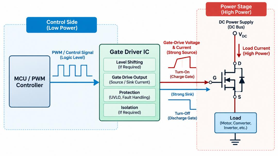
A gate driver is an interface component which is used between a controller and a power semiconductor switch (e.g., MOSFET, IGBT, SiC MOSFET, and Gallium Nitride devices). A gate driver takes input from a logic or PWM signal and outputs the necessary voltage and current for driving the gate of the power switching component. A gate driver performs various other tasks as well, depending on the requirement of the application (e.g., level shifting, timing, isolation, and protection). The gate driver does not carry the current of the load. Instead, the gate driver drives the switch which handles the current. Its position in the signal path can therefore be represented as:
MCU / PWM Controller → Gate Driver → Power Switch → Load
The term gate driver describes the function, while a gate driver IC is one common integrated implementation of that function. Gate-drive circuits can also be constructed using discrete components.
2.1 Where the Gate Driver Sits in the Power Stage
In a normal power electronic circuit, the control and power stages serve distinct purposes. In the control stage, the switching signal is produced depending on the mode of operation using the specific control algorithm. The signal could come from a microcontroller, DSP, FPGA, PWM controller, or other digital controller circuits. After being generated, the signal is fed to the gate driver, where the signal is processed. It is here that the signal gets processed through an increase in the available gate drive current, conversion into the right voltage level, shifting the signal to a floating reference point, or galvanic isolation of the control and power stages. The simplified signal chain is:
MCU / PWM Controller → Gate Driver Circuit → MOSFET / IGBT → Power Converter → Load
The difference between the two blocks is significant. The controller decides the timing of the power switch, whereas the gate driver makes the switching transition possible by providing the capacity for it. The MOSFET/IGBT does the power switching. Thus, in the case of a DC-DC converter, the controller will produce a PWM signal with some particular duty cycle. The gate driver receives the PWM signal and supplies the gate of the MOSFET with the proper voltage and current. Then, the MOSFET manages the energy transmitted in the converter.
For a high-side operation, the complexity of the driving block may increase since the source/emitter of the switching element changes its position with respect to the ground. Consequently, the driver will need a bootstrap supply, level shifting circuit, floating supply, or any other suitable high-side driving scheme. There might be a need for galvanic isolation in systems where control and power parts must remain electrically isolated from each other. The driver circuit thus becomes the interface between the low-power control electronics and power-switching blocks. While the driver controls the power semiconductor, it does not have to bear the load current itself.
2.2 Gate Driver IC vs. Discrete Gate-Drive Circuit
It is not always necessary that the gate driver should be an integrated circuit. The entire gate drive requirement can be achieved by using transistors, resistors, diodes, and logic devices, among others. Dedicated gate drivers ICs incorporate all these functionalities in a compact form and are often used in power conversion circuits.
A simplified comparison is shown below.
| Feature | Gate Driver IC | Discrete Gate-Drive Circuit |
|---|---|---|
| Implementation | Integrated semiconductor device | Individual transistors and passive components |
| Drive stage | Integrated output stage | Designed using discrete components |
| Gate-current capability | Specified by the IC datasheet | Determined by the selected components and circuit |
| Logic interface | Often integrated | Must be designed separately |
| Level shifting | Available in appropriate devices | Requires additional circuitry |
| Isolation | Available in isolated driver devices | Requires separate isolation components or circuits |
| UVLO/protection | May be integrated | Usually requires additional components |
| Design complexity | Generally lower | Generally higher |
| Flexibility | Defined by the IC architecture | High circuit-level flexibility |
| Datasheet dependence | Key electrical parameters are directly specified | Multiple component specifications must be considered |
The gate driver IC can have built into it the output stage for charging and discharging the gate of the power device, along with other capabilities such as UVLO, enable, level shifting, interlock, or protection depending upon the exact device. In other words, different devices may have different capabilities, which means that the corresponding data sheet needs to be consulted rather than assume that all gate driver ICs have identical capabilities.
Nonetheless, discrete gate driver circuits can be useful if the designer wants to use a specific drive feature, specific voltage/current capability, or a custom circuit. Discrete gate driver circuits also offer flexibility where a standard gate driver IC fails to meet the specified operating conditions. In any case, it needs to be remembered that the design of the entire drive circuit has to take into account various aspects including component tolerances, switch timings, drive impedance, parasitic inductance, voltage and protection.
Hence, the difference is that “gate driver” refers to the function, whereas “gate driver IC” is a common IC implementation of this function.
3. Why Do MOSFETs and IGBTs Need Gate Drivers?
Although MOSFETs and IGBTs are voltage-controlled power switches and draw very little steady-state gate current, their gates behave as capacitive loads during switching. Understanding how a MOSFET works, particularly its gate control and operating regions, helps explain why the gate must be charged to turn the device on and discharged to turn it off. Faster switching requires the driver to source and sink this gate charge more quickly.
In a basic MOSFET switch circuit, a microcontroller or PWM controller may generate the required HIGH and LOW commands but still lack the gate voltage, transient current, switching speed or high-side capability required by the power device. A MOSFET or IGBT gate driver solves this problem by charging and discharging the gate in a controlled manner.
3.1 The Limits of Driving a Power Switch Directly from a Controller
A controller can in some cases be used to drive a small MOSFET directly, especially when there are a low switching frequency and the gate charge is low. But as the power, frequency of switching, gate charge, or topology becomes difficult, direct connection of the controller becomes increasingly undesirable.
One major disadvantage is the current sourcing capability of the controller output. In switching transition, the controller has to either charge or discharge the MOSFET or IGBT gate. This produces transient rather than continuous gate current, and the peak current can be substantial. Thus, an output current that can satisfy a logic input may not necessarily be sufficient to charge the power device gate.
The second disadvantage is the necessary gate drive voltage. For example, a MOSFET can have a specific value of gate-to-source voltage while an IGBT has its own requirements of gate-emitter drive voltage. Even though a transistor can be operated by a specific logic signal, this does not imply that the device will operate with the intended conduction and switching behaviour. This can be determined from the datasheet of the specific power device.
High side switching poses an additional challenge as well. The reference point for the gate of a high-side MOSFET need not be the ground of the controller. With the switching point moving, the reference point for the source of the high-side MOSFET will move as well. The correct configuration for the high-side gate driver would be one which can produce the gate drive with respect to the source point of the MOSFET, not just the PWM signal with respect to ground of the controller.
Isolation can pose yet another requirement. In some power converters, the control circuitry and the power stage require galvanic isolation.
The difference can be summarized as follows:
| Direct Controller Drive | Gate Driver Drive |
|---|---|
| Controller directly charges and discharges the gate | Dedicated driver provides the gate current |
| Limited by controller output capability | Designed specifically for gate-drive requirements |
| Logic voltage may not match device requirements | Drive voltage is selected for the power device |
| High-side operation can be difficult | Appropriate high-side drive arrangements are available |
| Isolation requires additional circuitry | Isolated gate driver ICs are available |
| Less control over switching transition | Drive strength and external components can be designed for controlled switching |
Therefore, a controller being capable of turning a MOSFET ON under a static or low-speed test does not necessarily mean that it can drive the device reliably at the intended switching frequency and power level.
3.2 How Switching Speed Affects Loss, Heat, and Reliability
The speed of the transition process of the power semiconductor from ON to OFF state impacts the performance of the power stage. Thus, a gate driver should deliver an appropriate switching transition instead of trying to generate the most rapid gate edges.
When the gate charges and discharges slowly, the power semiconductor remains in its transition zone for a longer period of time. At this point, both voltage and current may become significant. As a result, the switching energy becomes a source of power loss.
Repeated at a switching frequency f(sw), the approximate relationship can be expressed conceptually as:
P(SW) ≈ E(SW) x f(SW)
Thus, longer switching time will cause increased switching losses and will lead to an increased device temperature. It is especially critical for converters that operate at high switching frequencies.
Nevertheless, higher switching frequency does not mean anything good. Increasing the drive level or decreasing the gate resistance will result in faster switching. However, very fast switching will lead to the increase of the rates of change of voltage and current (dv/dt and di/dt). These rates will cause interaction with the parasitic inductance and capacitance of the power and gate drive loops, resulting in oscillations and EMI.
Fast switching can cause parasitic effects due to the Miller effect of the power transistor. In certain cases, it may cause unwanted turn-on of another switch, especially in bridges.
The design objective is therefore a controlled switching transition:
Too slow → longer transition → higher switching loss → more heat
Too fast → higher dv/dt and di/dt → ringing, overshoot, EMI, and possible device stress
Controlled → appropriate switching loss with acceptable EMI and device stress
The gate driver, in conjunction with the power device parameters, the gate resistance, the PCB design, parasitic elements, and the switching configuration, is the factor that decides how the switching occurs in this trade-off.
That is the reason that a gate driver must not necessarily have to be chosen only because of the fact that it provides maximum drive current capability among other choices. While more drive current may reduce the transition times, it might increase ringing, overshoots, EMI, and stress on the device, if other components of the gate driver and the power circuit are not designed appropriately.
It is important to keep in mind that the main function of a gate driver is not to switch at its maximum possible speed, but rather it is intended to provide the switching action in a controlled manner.
4. How Does a Gate Driver Work?
A gate driver takes a relatively weak control signal generated by a controller and transforms it into a gate-drive signal that is appropriate for controlling a power semiconductor. In its most basic form, the process involved in a gate driver could be seen as a combination of signal reception, signal conditioning, turn-on gate charging, and turn-off gate discharging.
The components that make up a conventional gate driver include an input stage which receives the PWM or logic signal, a control or level shifting stage within the driver itself if need be, and an output stage which is capable of sourcing and sinking the current necessary for the gate of the power device.
The simplified operating path is:
PWM/Logic Input → Input/Control Stage → Gate-Drive Output Stage → Power-Switch Gate When the control input commands turn-on, the driver’s output stage supplies current to the gate, charging its capacitances. In case the control goes into the OFF state, then driver provides the discharge channel and releases the charges from the gate. The dynamics and form of these transitions depend on the driver, gate charge of power device, the external gate resistance, parasitic inductances and capacitances, and operating mode selection.
Internal structure differs from one type of the gate driver IC to another. Some chips are dedicated to low-side control, whereas other ICs offer high-side or half bridge control features. In isolated gate drivers, the isolation barrier is added between input and output parts of the chip. Consequently, internal block structure must always be analysed taking into account the driver and power device datasheet.
4.1 Basic Operating Principle
Let us consider that a MOSFET is attached to the output of a gate driver. Initially, the controller will produce a PWM signal indicating the desired switching command. The gate driver will receive this signal and will provide the proper output according to the reference point of the driver.
In case when the command at the input asks for turning on, then the output stage of the driver will sink current into the gate of the MOSFET. As a result, the gate charges and the gate to source voltage becomes close to the desired level. When the operation of the device becomes correct, then the MOSFET switches to its operational mode.
In case when the command at the input asks for turning off, then the driver will change its output and will sink current out of the gate of the MOSFET.
This process occurs repeatedly at the converter's switching frequency.
A simplified sequence is:
Turn-on command
Controller sends HIGH → Driver sources gate current → Gate charge increases → Gate voltage rises → Power switch turns ON
Turn-off command
Controller sends LOW → Driver sinks gate current → Gate charge decreases → Gate voltage falls → Power switch turns OFF
Therefore, the driver circuitry does not just replicate the waveform from the controller, but provides the current needed to move the gate charge quickly.
In case of a bridge converter, the driver may even have to synchronize multiple switching elements. The timing of such switching elements becomes important since it is possible to have both the switching devices turn on at the same time, thus creating a direct current path through the power source. Depending on the device used for gate driver ICs, it may have interlocking or controlled dead time circuits.
In case of a high-side switch, it is necessary that the gate be charged based on the voltage relative to the source/emitter of the switch and not the system ground. This may be achieved through a variety of methods, such as bootstrap configurations.
4.2 Source Current During Turn-On and Sink Current During Turn-Off
One of the most important characteristics of a gate driver is its ability to source and sink gate-drive current.
During turn-on, the driver sources current into the power-device gate. These current charges the gate and associated capacitances. A simplified relationship between gate charge and average gate current is:
I(G) ≈ Q(G) / t (SW)
where:
- I(G) is the approximate average gate current,
- Q(G) is the required gate charge,
- t(SW) is the desired switching time.
While this equation may be helpful in initial estimations, it is not recommended to use it as the actual predictor of the maximum output current of the driver. The real value of gate current depends on a number of factors including gate-charge curve of the power device, driver output impedance, external gate resistor, internal resistance of the device, parasitic inductance, and gate voltage at any moment of time.
At the end of turn-off process, the driver absorbs current from the gate. Gate charge is absorbed, and gate voltage goes to the necessary OFF state.
Gate drive sources and sinks do not have to be equal. In some applications, it makes sense to have a different sink and source impedance so that they could be controlled independently. It is especially true for bridge circuits, where a good turn-off capability can absorb gate charge quickly and decrease chances of false turn-on of the device due to voltage transients on its parasitic capacitances.
This is the reason why you need to check both source and sink current on the datasheet, and not just single gate current figure.
The basic current paths can be represented as:
Turn-on:
Driver supply → Output stage → Gate → Gate capacitance
Turn-off:
Gate → Output stage → Driver return
The gate resistor is normally located between the output of the driver and the gate of the power device. The gate resistor serves to provide impedance to the gate drive path and can be used for the regulation of the rate at which the gate charges and discharges.
4.3 Gate Charge, Miller Plateau, and Switching Time
The concept of gate charge is vital for comprehending the manner in which the gate drive controls a MOSFET/IGBT device.
Though the gate is usually considered as a capacitor, its capacitance is not fixed throughout the entire cycle of switching operation. Gate charge data is available in the device’s datasheet, which describes the dependence of the necessary gate charge on gate and drain/collector voltages under certain conditions.
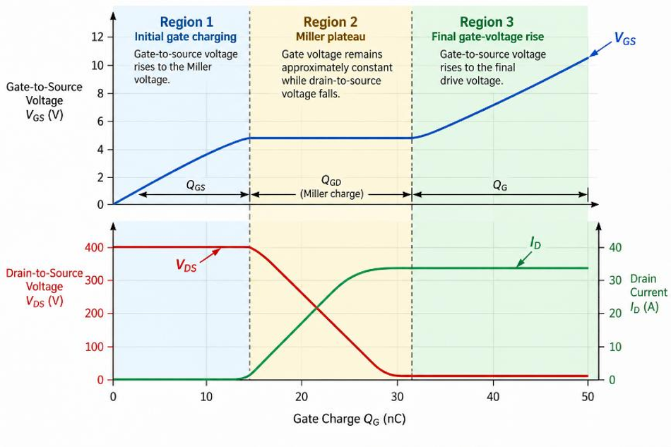
In a usual turn-on sequence, the gate voltage rises first, as the driver injects the charge into it. Then the power device starts approaching the range at which the change of the drain/source or collector/emitter voltage becomes significant. In that moment, the rise of the gate voltage may become slower, and be called the Miller plateau.
The simplified sequence is:
1. Gate charging begins – the driver supplies current to raise the gate voltage.
2. Initial device turn-on – the power device begins responding to the increasing gate voltage.
3. Miller plateau – a significant portion of the supplied gate charge is associated with the change in the device's switching voltage.
4. Final gate charging – the gate voltage continues toward its final drive level.
The Miller plateau is significant since it is directly related to the primary voltage change of the power device. The amount of the charge and the time needed to transfer this charge influence the switching process.
The gate charge switching time relationship can therefore be employed as an estimation of the gate drive requirement. However, the simple expression
I<sub>G </sub>≈ Q<sub>G </sub>/ t<sub>SW</sub>
does not completely describe the instantaneous current waveform. More realistic design assessment takes into account the full shape of the gate charge waveform, the driver source/sink impedance, the external gate resistance, the internal gate resistance, parasitic inductance and the actual gate drive voltage and current.
Therefore, the role of the gate driver is to balance between proper drive and proper switching. Increasing the drive strength decreases the transition time, however too much aggressiveness in driving the gate can cause excessive ringing and overshoot and increases EMI and stress on the device. On the other hand, too little drive causes unnecessarily long switching transitions with excessive switching losses.
In practice, it is necessary to take both the driver and the power device datasheets into consideration for the design. The driver should be capable of delivering the needed voltage and source/sink currents while the gate drive circuit delivers a suitable switching waveform.
5. Main Types of Gate Drivers
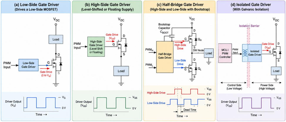
Gate drivers may be categorized based on the position of the power switch in the circuit, number of switches under control and if the control and power sections are electrically isolated or not. The most common gate drivers include low side gate drivers, high side gate drivers, half bridge/Full bridge gate drivers, and isolated gate drivers.
Selection of the appropriate gate driver is dependent mainly on the switching topology and the ground reference of the power switch. For instance, a high-side switch does not have to be driven like a low-side switch at all times since the source/emitter might change its reference level from ground. Bridge converters need to have coordinated switching control, while isolated power converters may demand that the control and power stages be electrically isolated.
The major types are summarized below.
| Gate Driver Type | Typical Configuration | Main Characteristic | Common Applications |
|---|---|---|---|
| Low-side driver | Switch connected on the low side | Gate referenced to a relatively fixed ground/source node | Buck converters, low-side switching, motor control |
| High-side driver | Switch connected on the high side | Gate must be driven relative to a moving source/emitter node | Buck converters, half-bridges, motor drives |
| Half-bridge/full-bridge driver | Two or more coordinated switches | Provides multiple synchronized gate-drive outputs | Inverters, motor drives, DC-DC converters |
| Non-isolated driver | Input and output share an electrical reference or use a non-isolated interface | Simpler signal path | Many low-voltage and grounded power stages |
| Isolated driver | Control and power sides are galvanically separated | Provides electrical isolation between domains | High-voltage converters, industrial systems, isolated power stages |
5.1 Low-Side Gate Drivers
The gate driver in case of low side configuration drives a switching device whose source or emitter is connected to a fairly stable reference point like the circuit ground or return path.
The voltage between gate and source/emitter being known with respect to a stable reference point makes the drive simpler compared to the floating high side drive configuration.
A simplified arrangement is:
Controller → Low-Side Gate Driver → MOSFET/IGBT → Load
In the case of a low-side MOSFET, the driver provides the proper voltage for the gate with respect to the source for turn-on, and the gate is brought down to the source for turn-off. The controller and driver have the same reference if isolation is not required.
Low-side drivers are frequently used in applications such as:
- DC-DC converters
- Low-side load switching
- Motor-control circuits
- Power supplies
- Battery-powered switching systems
- General-purpose PWM switching stages
Low-side drive can also be advantageous where the power switch may be located between the load and the circuit return path. However, proper selection of the driver must take into account the specifications for the MOSFET or IGBT, frequency of switching, and drive current required.
Although the low-side drive has a simple design, it does not mean that the issue of layout and switching performance is not important. There are still inductances and resistances present in the drive loop, and the inappropriate drive strength or gate resistance may cause ringing.
5.2 High-Side Gate Drivers
A high-side gate driver drives the power switch placed on the high side of the power stage. Here, the source of the high-side MOSFET and the emitter of the IGBT vary in relation to the circuit ground, depending on the switching state of the switching node.
In such a case, the gate-drive signal needs to be generated relative to the source/emitter of the power transistor and not just relative to the controller ground.
A simplified high-side arrangement is:
Controller → High-Side Gate Driver → High-Side MOSFET/IGBT → Load
The driver therefore requires a suitable method for generating or transferring the gate signal to the floating switching node.
Several approaches can be used depending on the topology and application. These can include:
- Bootstrap-based high-side drive
- Level-shifting circuits
- Floating gate-drive supplies
- Isolated gate-drive arrangements
- Other topology-specific drive techniques
It is therefore not correct to assume that every high-side switch requires an isolated gate driver. Isolation is one possible approach, but bootstrap and other floating-drive methods are also widely used.
High-side gate drivers are commonly found in:
- Half-bridge converters
- Synchronous buck converters
- Motor drives
- Inverter stages
- Automotive and industrial switching systems
- High-side power-switching circuits
When choosing a high-side driver, it is necessary to confirm the necessary high-side supply configuration, operating voltage, switching frequency, and any duty cycle restrictions as well as its capability to provide the needed gate-source voltage in operation.
For circuit examples showing how channel type affects gate-drive requirements, compare N-channel and P-channel MOSFET configurations.
5.3 Half-Bridge and Full-Bridge Gate Drivers
Most power converters need more than one switch. A half bridge generally comprises two switches in series with each other between the DC source. A full bridge is made up of two switching legs, thus having four switching devices.
As these switches work in a coordinated fashion, the corresponding gate driver needs to supply control signals accordingly.
A simplified half-bridge arrangement is:
High-Side Driver → High-Side Switch
Low-Side Driver → Low-Side Switch
with both switches connected around a common switching node.
Both switches should not normally be switched on at the same time. In case both are conducting simultaneously, a low impedance path can result between the supply rails, which will lead to the occurrence of shoot-through. The latter phenomenon results in high transient current and may damage the switching devices.
For this reason, half-bridge and full-bridge gate drivers may incorporate features such as:
- High-side and low-side outputs
- Level shifting
- Interlocking
- Dead-time control
- Bootstrap support
- UVLO
- Enable or shutdown functions
- Fault handling, depending on the device
The exact features vary between gate driver ICs and must be confirmed from the datasheet.
Half-bridge and full-bridge drivers are widely used in:
- Motor drives
- DC-AC inverters
- Synchronous converters
- Resonant converters
- Battery power converters
- Renewable-energy power converters
- Industrial power supplies
The key selection issue is not simply the number of outputs. The designer must ensure that the driver's timing, high-side supply method, output current capability, and protection features are appropriate for the selected switching devices and operating frequency.
5.4 Isolated vs. Non-Isolated Gate Drivers
Another essential criterion here is the presence of galvanic isolation between the controlling side and the power device side of the gate drive signal.
When the gate driver is non-isolated, there is no galvanic isolation between the input and the output parts of the driver. Hence, the references for the respective circuits are connected in accordance with the particular driver topology.
Non-isolated drivers are usually employed when the control and the power sides can share the electrical reference. They offer a fairly simple signal path.
Isolated gate drivers contain an isolation barrier between their input and output parts. The control signal is transmitted across the barrier, while the two sides are electrically separated.
Isolation can be useful when:
- The power stage operates at a substantially different potential from the controller.
- The controller must be protected from high-voltage transients.
- Multiple power stages operate at different electrical potentials.
- The system architecture requires galvanic separation.
- Ground-potential differences could otherwise interfere with the control signal.
The major parameters for an isolated gate driver IC include isolation capability, common mode transient immunity (CMTI), propagation delay time, channel matching, drive capability, and the power source for the isolated side.
Common Mode Transient Immunity is especially important for fast switching systems since the switching node is subject to a relatively large common mode voltage transition in a very short period of time.
The following comparison summarizes the distinction:
| Characteristic | Non-Isolated Gate Driver | Isolated Gate Driver |
|---|---|---|
| Galvanic isolation | No | Yes |
| Circuit complexity | Generally lower | Generally higher |
| Control/power reference | Electrical relationship required | Input and output electrically separated |
| Typical use | Common-reference power stages | High-voltage or electrically separated systems |
| Important parameters | Drive current, voltage, timing, UVLO | Isolation, CMTI, delay, drive current, supply |
| Power supply requirements | Generally simpler | May require isolated output-side supply |
The decision to use isolated and non-isolated operation needs to come from the electrical architecture of the system and not merely from the voltage level of the power switch. Isolation might be required for a high voltage application but the need for isolation will finally depend on factors like the system’s architecture, safety architecture, grounding and the transient environment.
Choosing the Appropriate Gate Driver Type
The classification above provides a practical starting point for selecting a gate driver:
Step 1: Switching Position. Define the power switch: low-side switch, high-side switch, or bridge circuit.
Step 2: Number of Controlled Switches. Single switch topology would need only one driver channel, half/fully bridge topology needs multiple controlled switches.
Step 3: Reference Configuration. Define if the driver can use common reference with the controller, or power circuit requires galvanic isolation.
Step 4: Power Device Requirements. The driver must be compatible with selected MOSFET, IGBT, SiC MOSFET, GaN or other transistor and its gate drive requirements.
Step 5: Timing and Drive Capability. Driver must be capable of sourcing/sinking required amount of current, have required propagation delay, switching frequency, dead time, high-side operation limits.
This approach helps the designer make an initial choice of gate-driver architecture before evaluating individual gate driver ICs. The second step will be defining driver compatibility with specific power switch technology: MOSFET, IGBT, SiC or GaN.
6. Matching a Gate Driver to MOSFET, IGBT, SiC, or GaN
Choosing a gate driver starts with finding out what power semiconductor the driver should drive. Even though MOSFETs, IGBTs, Silicon Carbide MOSFETs, and Gallium Nitride transistors all have a gate-controlled switch, they do not have exactly the same electrical parameters and switching needs. As a result, the fact that some particular gate driver functions correctly with one power semiconductor doesn’t mean that it will function correctly with another.
The right way to choose the gate driver is to start from the datasheet of the power semiconductor and find out the gate-drive needs of that particular power semiconductor.
The major considerations are summarized below.
| Power-device technology | Main gate-drive consideration | Important parameters to examine |
|---|---|---|
| Silicon MOSFET | Efficient charging and discharging of gate charge | Gate voltage, total gate charge, source/sink current, switching frequency |
| IGBT | Appropriate gate-emitter drive and controlled switching | Gate voltage, gate charge, source/sink current, switching timing |
| SiC MOSFET | Fast switching with careful control of voltage, ringing, and EMI | Specified gate-drive voltage, gate charge, source/sink current, negative-bias requirements where specified, CMTI for isolated designs |
| GaN transistor | Precise, fast gate control with close attention to device-specific limits | Gate-drive voltage range, timing, source/sink capability, parasitics, maximum gate voltage |
These classifications should not be considered universal guidelines for voltages and currents but rather only a beginning point in designing. The permissible gate drive conditions can differ greatly from one device to another, even for the same semiconductor process.
6.1 Matching a Gate Driver to a Silicon MOSFET
A typical silicon MOSFET is operated by applying the proper voltage between its gate and source. The gate need not draw any appreciable amount of current under normal operating conditions, although the driving circuit must keep charging and discharging the gate capacitance of the MOSFET.
For a MOSFET gate driver, the designer should examine:
- Required gate-to-source voltage
- Total gate charge QGQ_G
- Gate-charge curve
- Internal gate resistance
- Desired switching time
- Required source and sink current
- Switching frequency
- Maximum allowable gate voltage
- Driver output resistance
- PCB parasitic inductance
The total gate charge is especially valuable in this case since it gives an indication of how much charge must be moved in the course of a switching action, compared to merely measuring one particular capacitance value.
For a rough calculation of the gate current, the average gate current could be equated with the gate charge and desired switching time:
I(G) ≈ Q(G) / t(SW)
Nevertheless, this must not be seen as an exact peak current requirement. Gate current waveform depends on the driver’s output impedance, external gate resistor, MOSFET gate resistance, gate charge characteristics, and parasitics.
Thus, an appropriate gate driver IC should be chosen by matching these requirements with the driver’s datasheet specification.
6.2 Matching a Gate Driver to an IGBT
The IGBT also has a gate lead for controlling conduction, but its switching characteristics are not the same as those of a typical MOSFET. The choice of gate driver, therefore, is made depending on the drive characteristics specified by the IGBT manufacturer.
Important parameters include:
- Required gate-emitter voltage
- Total gate charge
- Gate-drive current
- Turn-on and turn-off requirements
- Switching frequency
- Propagation delay
- UVLO behaviour
- Protection requirements where applicable
In terms of high-power applications, gate drive ICs for IGBTs may contain additional protection features. Depending on the specific application, features like desaturation detection, fault indication, soft turn-off or Miller-clamp functionality may be relevant. Application and device-specific features like these should never be taken for granted in every gate drive IC for IGBTs. The turn-off must be controlled as well by the gate drive. When considering a high-power switching system, an uncontrolled or excessive turn-off could result in additional switching losses, whereas an overly aggressive transition would lead to voltage overshoot and electromagnetic interference.
Hence, the goal here is controlled switching once more, and not maximum gate drive current.
6.3 Matching a Gate Driver to a SiC MOSFET
SiC MOSFETs are capable of fast switching and operating at higher voltages and therefore suitable for use in high-performance power conversion systems. The ability to switch places much more focus on the performance of the gate drive circuit used.
In choosing a gate driver for a SiC MOSFET, the engineer needs to check for the exact gate voltage required from the SiC MOSFET data sheet, and not just take any arbitrary gate drive voltage because of its use by another MOSFET or another SiC component.
Important considerations include:
- Specified gate-drive voltage range
- Total gate charge
- Required source and sink current
- Switching speed
- Gate resistance
- Parasitic inductance
- Voltage overshoot and ringing
- Common-mode transient immunity for isolated drivers
- UVLO characteristics
- Required protection functions
- Negative gate bias, if specified by the particular device and application
The combination of high switching speed with low parasitic inductance is especially crucial in SiC devices. High drive strength enables rapid transitions of the gate but can also cause more ringing, overshoots, electromagnetic interference (EMI), and stress to the transistor.
Hence, choosing a drive with the highest possible current capability is not a good design approach. The drive, gate resistance, layout, power transistor, and application conditions have to be taken into consideration together.
When comparing SiC MOSFETs, use each device’s datasheet to confirm its gate-drive requirements before choosing a driver.
6.4 Matching a Gate Driver to a GaN Device
GaN components may have very fast switching transitions; however, their gate-drive characteristics may depend greatly on particular transistor technologies and suggested operational parameters of particular manufacturers.
Thus, the datasheet of the particular GaN component should be used as the main source of information about gate-drive voltages and operating limits. It must be noted that gate-voltage tolerances and drive parameters may vary greatly from one GaN component to another; thus, a gate-driver which suits a certain GaN transistor may not suit another.
Important considerations include:
- Device-specific gate-voltage range
- Maximum allowable gate voltage
- Required drive current
- Switching frequency
- Propagation delay
- Driver-to-device loop inductance
- PCB parasitics
- Input and output timing
- Noise immunity
- Required protection functions
As GaN switching transitions are very rapid, even slight parasitic components in the gate drive circuit may affect the shape of the waveform. Placement of the driver and the power device, gate loop layout, gate impedance, and return paths may become significant in this design. The selection principle remains the same: the driver must be compatible with the particular GaN device rather than being selected solely from the general label "GaN gate driver."
6.5 Key Differences When Matching Driver and Power Device
The following table provides a practical comparison.
| Parameter | Silicon MOSFET | IGBT | SiC MOSFET | GaN |
|---|---|---|---|---|
| Gate control | Voltage-controlled | Voltage-controlled | Voltage-controlled | Voltage-controlled |
| Gate charge | Must be charged/discharged during switching | Must be charged/discharged during switching | Important because of fast switching | Particularly important for fast switching |
| Drive voltage | Follow MOSFET datasheet | Follow IGBT datasheet | Strictly follow SiC datasheet | Strictly follow GaN datasheet |
| Drive-current requirement | Depends on Q<sub>G</sub> and switching time | Depends on Q<sub>G</sub> and switching time | Often important for fast transitions | Highly dependent on device and switching conditions |
| Timing | Important | Important | Very important | Very important |
| Parasitic effects | Important | Important | Can become significant with fast switching | Particularly sensitive in fast-switching designs |
| Protection | Application-dependent | May require additional fault functions | Application-dependent | Device-specific |
| Driver selection basis | Device + topology + switching requirements | Device + topology + switching requirements | Device + topology + high-speed switching requirements | Device + topology + device-specific gate limits |
6.6 A Practical Matching Procedure
One can successfully couple a power transistor with a gate driver if one works from the power transistor backward towards the gate driver.
Step 1: Establish the actual power transistor. Find out whether the switch is a silicon MOSFET, IGBT, SiC MOSFET, or GaN and get the data sheet.
Step 2: Find out the recommended gate driving conditions. Find out the recommended gate-source or gate-emitter voltage.
Step 3: Find out the gate charge. Get from the data sheet information about the gate charge.
Step 4: Determine the switching speed. Define the needed ON/OFF switching speed.
Step 5: Determine the drive capability. Estimate the needed drive capability, using gate charge and switching speed, but remember that the actual peak current will depend on the whole drive circuit.
Step 6: Check the topology. Decide whether the power device is low side, high side, half bridge, or something else.
Step 7: Isolation Requirements. Find out whether a non-isolated gate driver is suitable or galvanic isolation is necessary.
Step 8: Check Timing and Protection. Check propagation delay, channel matching if applicable, UVLO, dead time or interlocking capabilities, CMTI if isolator is used, and other necessary protections.
Step 9: Physical Gate-Drive Circuit. Verify gate resistance, decoupling, return current, loop inductance, and PCB design.
The key concept is that the power semiconductor switch and the gate drive should be considered as a matched pair. Gate drive should meet the electrical specifications of the chosen device and topology, while gate drive circuit itself should deliver the desired switching waveform in real-life conditions.
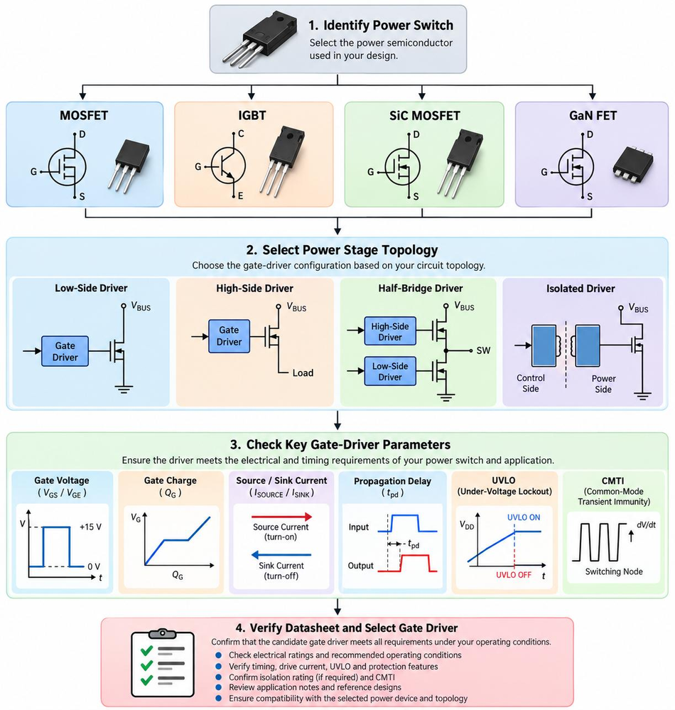
7. Key Gate Driver Specifications and Selection Steps
Selection of a gate driver needs to start with the specifications of the power switch and the switching technology and not with a particular specification, for example, the maximum output current. The right driver has to meet both the gate voltage specifications as well as those of timing, isolation, and protection.
The selection process can be viewed as a sequence:
Power Switch → Topology → Isolation → Drive Voltage → Source/Sink Current → Timing → Protection → Layout and Verification
The most important specifications are discussed below.
7.1 Start with the Power Switch, Topology, and Isolation Requirement
The first step is to identify the exact power semiconductor that the driver will control. The device may be a silicon MOSFET, IGBT, SiC MOSFET, or GaN device. Its datasheet provides the fundamental gate-drive requirements that the driver must satisfy.
The following information should be collected before selecting the driver:
- Power-device type
- Required gate-to-source or gate-to-emitter voltage
- Total gate charge
- Maximum gate voltage
- Desired switching frequency
- Required switching time
- Internal gate resistance, where specified
- Low-side or high-side position
- Half-bridge or full-bridge configuration
- Required isolation
- Operating temperature and supply conditions
The switching topology must then be considered. In general, the low-side switch will have simpler reference considerations, while the high-side switch could require either a floating or a level-shifted driver. The half-bridge could call for combined high-side and low-side outputs, while the full-bridge needs more than one switch output channel.
Isolation is a completely independent consideration. If the controller and power stage need to be electrically separated from each other, an isolated driver might be the solution. On the other hand, if they can use the same reference in a safe way, a non-isolated driver would do. One should not rely exclusively on the power switch voltage level when selecting the gate driver. The driver does not have to bear the load current. It simply drives the power switch gate, and hence, its compatibility would depend on different factors.
7.2 Drive Voltage, Source/Sink Current, and Gate Charge
Once the power device has been identified, the next step is to compare its gate-drive requirements with the driver's output specifications.
Gate-drive voltage
It is essential that the gate driver provides a voltage level suitable for the chosen power device. Gate voltage required and maximum gate voltage that can be used need to be taken from the datasheet of the power device.
This is especially true when it comes to devices made up of silicon carbide and gallium nitride because gate voltages for different devices belonging to the same semiconductor material may vary.
Source and sink current
The driver must be capable of supplying and removing the required gate current.
During turn-on, the driver sources current into the gate to charge it. During turn-off, it sinks current from the gate to remove the stored charge.
A preliminary estimate can be obtained from:
I(G) ≈ Q(G) / t(SW)
For example, if a device has a specified gate charge Q_G and the designer wants that charge moved within a particular switching interval, the equation provides an initial indication of the required gate-drive capability.
Nevertheless, this is just an initial approximation. The actual maximum value of gate current depends on the output impedance of the driver, gate resistor, gate impedance, gate charge parameters, parasitic inductance, and instantaneous operating point.
Source and sink specifications should thus be considered individually. A driver with high source current specification does not necessarily offer equally high sink current capacity.
Gate charge
Gate charge can prove more useful in choosing a proper driver than simply considering a single value of input capacitance. The gate-charge plot given in the datasheet provides information concerning distribution of charge during the switching transition.
Higher values of gate charge generally imply higher amounts of charge that have to be transferred during each switching process. At any given switching frequency, this will affect the energy consumed in charging and discharging the gate.
A preliminary estimate of average gate-drive power can be related to gate charge, drive voltage, and switching frequency:
P(G) ≈ Q(G) V(G) f(SW)
This expression is useful as an initial estimate, but actual driver power consumption also depends on the driver's internal operating current, charging/discharging paths, switching conditions, and circuit architecture.
7.3 Timing, Noise Immunity, and Protection
The drive strength is just one factor to consider in selecting a gate driver. Timing and protection requirements may be equally important, especially for bridge circuitry and fast-switching devices.
Propagation Delay
Propagation delay is the delay between when an input on the gate driver changes state and when the output on the driver changes state.
A large or uncontrollable propagation delay may cause a problem with the timing of the power switch.
In applications that have more than one channel, the difference in the delays between the channels can also cause synchronization problems.
Dead time
For complementary switching circuitry, there can be a need for appropriate non-overlapped turn off of one switch and turn on of the other to avoid shoot-through.
The necessary dead time varies depending upon the type of power devices used, delays of the driver circuits, switching performance, conditions and the general topology of the system. The dead time needs to be evaluated from the overall switching system and not a universal fixed value.
Noise Immunity
Large transients of voltages and currents are developed in the process of operation of the power converter circuits. The gate driver should operate appropriately in spite of the noise produced in the switching section.
For isolated gate drivers, common mode transient immunity (CMTI) is a key parameter. It defines the performance of the gate driver under rapid change of common mode voltage across the isolation barrier.
This becomes particularly relevant in high-dv/dt switching applications.
Undervoltage lockout
The UVLO acts to inhibit gate driver operation if the supply voltage drops below an adequate value.
This will assist in ensuring that the power device is not driven at an inappropriate gate voltage. The parameters associated with the UVLO operation must be verified with respect to the chosen power device and system operation.
Protection functions
Depending on the application, useful driver features may include:
- UVLO
- Enable or shutdown input
- Interlocking
- Fault reporting
- Overtemperature protection
- Desaturation detection for applicable IGBT systems
- Miller-clamp functionality where appropriate
- Soft turn-off
- Short-circuit protection
Not every gate driver includes all of these features. They should therefore be treated as application-specific requirements and verified directly from the driver datasheet.
Gate Driver Specifications at a Glance
| Specification | Why It Matters | What to Check |
|---|---|---|
| Gate-drive voltage | Determines whether the power device is driven correctly | Recommended and maximum gate voltage |
| Source current | Controls gate charging during turn-on | Peak/source current rating |
| Sink current | Controls gate discharge during turn-off | Peak/sink current rating |
| Gate charge | Determines charge that must be moved | Q<sub>G</sub> and gate-charge curve |
| Propagation delay | Affects switching timing | Input-to-output delay |
| Channel matching | Important for multiple channels | Delay difference between channels |
| Switching frequency | Determines required dynamic performance | Driver and device operating limits |
| UVLO | Prevents unsuitable low-supply operation | UVLO thresholds and behaviour |
| CMTI | Important for isolated high-dv/dt systems | CMTI rating |
| Isolation | Separates control and power domains | Isolation specifications |
| Dead-time/interlocking | Helps manage complementary switching | Integrated or external implementation |
| Protection features | Helps manage fault conditions | Features required by the application |
7.4 Practical Gate Driver Selection Process
Once the necessary specifications are known, the process below may be followed to narrow down suitable gate drive ICs.
Step 1: Identify the power semiconductor
Start with the exact type of MOSFET, IGBT, SiC MOSFET or GaN device. Note down the recommended gate drive voltage, gate charge, maximum gate voltage and switching capability.
Step 2: Identify the switching topology
Identify if the semiconductor is used as a low-side switch, high-side switch, half bridge, full bridge or other configuration.
Step 3: Identify the reference topology
Identify how the references for input and output of the driver are defined. Identify if a floating high-side reference, level-shifting, bootstrap power supply or isolation is needed.
Step 4: Gate drive voltage check
Make sure that the voltage output of the driver is within the range of the power device's datasheet. Do not just pick the driver by looking at the logic voltage level of the controller.
Step 5: Gate current estimation
Based on the gate charge of the power device and required switching time, make an estimation. Compare the estimation with the source and sink capabilities of the driver, taking into consideration both external and internal impedance.
Step 6: Check timing
Compare the following factors with the intended application: propagation delay, channel-to-channel matching, dead-time requirements, and switching frequency.
Step 7: Check noise and isolation requirements
For isolated devices, check isolation parameters and CMTI. For non-isolated devices, check the common reference configuration of the driver.
Step 8: Check protection requirements
Determine the required types of protection for the intended application and check whether these are provided in the chosen driver.
Step 9: Check supporting components
The driver must be considered along with gate resistor, bypass capacitors, bootstrap components when appropriate, and gate return path. These components affect the real switching waveform.
Step 10: Check the complete design
The final choice should be verified using the power device datasheet, driver datasheet, application information, and switching waveforms measurement. Important parameters to check are the gate-to-source or gate-to-emitter voltage, drain-to-source or collector-to-emitter voltage, ringing at the switching node, overshoot, switching time, and driver supply.
Gate Driver Selection Checklist
Before finalizing a gate driver IC, the following checklist provides a practical verification point:
- Power semiconductor identified
- Recommended gate-drive voltage verified
- Maximum gate voltage verified
- Gate charge obtained from the device datasheet
- Required switching time established
- Source current checked
- Sink current checked
- Low-side/high-side configuration identified
- Half-bridge/full-bridge requirements identified
- Isolation requirement established
- Propagation delay checked
- Dead-time/interlocking requirements checked
- UVLO behaviour checked
- CMTI checked where applicable
- Required protection functions verified
- Gate resistor and decoupling requirements considered
- PCB gate-drive loop considered
- Switching waveforms planned for verification
This method of selecting a driver would then be referred to as device-based and topology-based. It is recommended that the designer does not pick a gate driver based on the current it can supply, but instead confirms whether the gate driver meets all the specifications. This is because there are many cases where the driver will appear powerful enough but will not result in the needed switching.
With these requirements defined, review candidate gate driver ICs and check their datasheets against your voltage, current, timing, and protection needs.
8. Practical Gate-Drive Design Checks
Choosing the appropriate gate driver is just the first part of ensuring reliable switching. The functionality of the entire gate-drive circuit is also influenced by the gate resistor, dead time, bootstrap circuit, if any, supply decoupling, PCB design, parasitic inductance, and the switching waveforms themselves.
The gate driver might have appropriate voltages and currents specified in theory but still show too much ringing, overshooting, EMI, or switching losses because of poor design of the surrounding circuitry. Verification thus needs to look at all parts of the switching system – gate drive, power device, passive components, and PCB design.
The following checks provide a practical starting point before moving to detailed power-stage optimization.
8.1 Gate Resistor, Dead Time, Bootstrap, and Decoupling
Gate resistor
The gate resistor is the easiest and most versatile component that controls the characteristics of a gate drive circuit by adding impedance between the driver output and power device gate, thus affecting the rate at which the gate is charged or discharged.
A lower value of the gate resistor will allow for greater gate current, and hence lead to faster switching. On the other hand, very low values will make the transition very aggressive, leading to ringing, overshoot, EMI, and inductance effects.
High gate resistance will result in low gate drive current, hence a slower switching transition. High resistance will reduce ringing and EMI in some cases, but will lead to increased switching losses due to longer time spent between the ON and OFF states.
The practical objective is therefore not simply to minimize the gate resistance. It is to select a value that produces an acceptable balance among:
- Switching loss
- Switching speed
- Voltage and current overshoot
- Ringing
- EMI
- Device stress
- Thermal performance
The correct value is based on the type of power switch used, driver output impedance, gate impedance of the transistor, board capacitance, operational voltage, switching frequency, and required switching response.
In bridge configurations, it could also prove advantageous to have separate turn-on and turn-off resistance values where such an arrangement is possible. This allows for more control over the two transitions.
Dead time
In a half bridge or full bridge configuration, there needs to be proper coordination between the high-side and low-side switches. There could be a delay created before switching the other switch ON after switching the first one OFF. This delay is referred to as dead time.
The role of the dead time is to ensure that there is a decreased probability of overlap in the operation of both the switches, resulting in a path across the source being created by the switching devices.
However, the dead time should not be too high. Large dead time could create extra conduction losses as the current could find another path during the switching cycle.
The required value depends on factors such as:
- Driver propagation delay
- Power-device turn-on and turn-off times
- Device gate charge
- Driver source and sink capability
- Temperature
- Operating voltage
- Load current
- Topology
Thus, dead time needs to be obtained by considering the switch behaviour of the whole system and not taking it as a constant universal value.
Bootstrap Considerations
The gate driver for high side is generally designed using bootstrap configuration to deliver a floating supply to the high-side driver circuit. The bootstrap circuit is usually designed with the help of diode or an integrated charging path with capacitor in order to obtain the high-side supply.
When a bootstrap-based driver is considered, the designer should verify:
- Bootstrap supply-voltage requirements
- Bootstrap capacitor requirements
- Charging conditions
- High-side operating duty cycle
- Switching frequency
- Leakage and quiescent-current effects
- Bootstrap diode or integrated charging-path characteristics
- Required high-side gate-drive voltage
Bootstrap functioning is topology-specific. The high-side power supply needs to be refreshed properly, and some operational cases would restrict the duty cycle.
For a given bootstrap configuration, a gate driver needs to be chosen from its respective datasheet and not based on the arbitrary choice of any bootstrap capacitor.
Decoupling
Gate drivers may generate transient current pulses during the charging and discharging of a power device gate. The supply side of decoupling circuitry needs to be placed in such a way as to have a low impedance path for current flow.
A decoupling or bypass capacitor needs to be placed close to the power connections on the driver.
PCB trace distances from the capacitor to the driver will add inductance to the system, which can reduce the performance of the local power supply network under current transients.
The appropriate values of capacitors will be found from the driver datasheets.
A practical gate-drive supply path can therefore be viewed as:
Driver supply → Local decoupling capacitor → Driver output stage → Gate resistor → Power-device gate
The return path should also be kept short and controlled.
8.2 PCB Layout and Waveform Verification
Gate-driver performance is strongly affected by PCB layout. This becomes increasingly important as switching transitions become faster because even small parasitic inductances can produce significant transient voltages.
A simplified relationship is:
V(L) = L di/dt
where:
V(L)is the voltage generated across a parasitic inductance,
L is the parasitic inductance,
di/dt is the rate of change of current.
With an increasing rate of change of switching current, the voltage produced by parasitic inductances increases.
Gate drive loop should be short
The loop constituted by the driver output, gate resistance, power device gate, and gate return should be short wherever possible.
A longer gate drive loop creates an increase in parasitic inductance. In case of fast switching, this inductance will resist the flow of gate current and cause voltage transients. Therefore, the driver should be located near the power semiconductor wherever possible.
Separate high-current power loops from sensitive control paths
There are rapid current changes possible within the gate drive loop and the switching loop as well. These should be taken into consideration in terms of their layout in order to prevent coupling of unwanted noise via high di/dt power lines.
Layout considerations should allow for proper gate current return path, while avoiding common impedances between the high-current switching loops and sensitive controls.
Minimize common-source or common-emitter inductance where appropriate
The source/emitter lead, which serves as the gate drive reference for an MOSFET or IGBT, may encounter voltage transients due to parasitic inductances.
The ideal layout must then reduce inductance that is unnecessary within the gate return path as well as adhere to the suggested layout techniques from the power device manufacturer when available.
Place decoupling close to the driver
The supply capacitance for the driver needs to be placed near the driver supply and return pins because of the current loop generated during the charging of the output stage and the gate of the power device.
For fast-switching devices, the distance between the driver, decoupling elements, gate resistance, and power device makes an impact on the switching waveforms.
Waveform Verification
A gate-drive circuit should not be considered fully validated simply because the circuit operates and the power device switches.
The actual waveforms should be examined during testing.
Useful measurements include:
| Waveform/Parameter | What It Helps Verify |
|---|---|
| Gate-to-source voltage V<sub>GS</sub> | Correct gate-drive voltage and switching behaviour |
| Gate-to-emitter voltage V<sub>GE</sub> | IGBT drive conditions |
| Drain-to-source voltage V<sub>DS</sub> | MOSFET switching transition and overshoot |
| Collector-to-emitter voltage V<sub>CE</sub> | IGBT switching behaviour |
| Switching-node voltage | High-side/half-bridge transition behaviour |
| Gate ringing | Gate-loop parasitics and stability |
| Voltage overshoot | Power-loop inductance and switching speed |
| Turn-on/turn-off time | Actual switching performance |
| Driver supply voltage | Supply stability during gate-current transients |
For the testing of rapidly changing gate signals, the test equipment itself may affect the signal measured. Connections of the probe via ground leads may add extra inductance, resulting in ringing, which may not be representative of the actual signal. Proper testing methods and short connections are thus essential when checking rapid switching waveforms.
A Practical Gate-Drive Verification Sequence
A systematic verification process can be useful:
1. Verify the driver supply. Confirm that the driver's supply remains within its specified operating range during switching.
2. Check the gate waveform. Measure the gate-to-source or gate-to-emitter voltage and verify that it reaches the required levels.
3. Check turn-on and turn-off transitions. Determine whether the switching times are consistent with the design target.
4. Look for excessive ringing. Inspect the gate waveform and switching-node waveform for high-frequency oscillations.
5. Check overshoot and undershoot. Verify that transient voltages remain within the power-device and driver limits.
6. Verify dead time in bridge circuits. Confirm that complementary switches do not overlap in a way that creates unacceptable shoot-through risk.
7. Check thermal behaviour. Measure device and driver temperatures under representative operating conditions.
8. Repeat under relevant operating conditions. Switching behaviour can change with input voltage, load current, switching frequency, and temperature, so verification should not be limited to a single operating point.
These design checks show that the gate-drive circuit must be evaluated at the system level. Gate resistance, dead time, bootstrap operation, supply decoupling, and PCB layout must be chosen to suit the selected driver and power device. Switching waveforms should then be checked to verify the complete design.
9. Common Gate Driver Applications
The gate drivers are employed in many power electronics applications because in the majority of cases there is a need for a controlled interface between the PWM controller circuitry and the power semiconductor. The choice of the correct gate driver depends on the particular switching topology, semiconductor type, voltage level, switching frequency, and electrical isolation requirements.
Some examples of typical applications can be DC-DC converters, motor drives, DC-AC inverters, renewable energy converters, battery charging/energy storage systems, industrial power supplies, and other high-frequency switching circuits.
9.1 DC-DC Converters
MOSFET drivers are commonly employed in DC-DC converters for switching MOSFETs, IGBTs, and other power switches.
A conventional DC-DC converter circuit includes a controller that creates a PWM waveform based on the desired output voltage or current. Gate driver then takes the PWM waveform and drives the switch with gate currents.
For instance, a buck converter may have a high-side or low-side MOSFET configuration. For driving the high-side MOSFET, a proper high-side driving method is needed, whereas for low-side MOSFET, a ground-referenced driving scheme could suffice.
Gate drivers in DC-DC converters help provide:
- Rapid gate charging and discharging
- Controlled switching transitions
- Appropriate gate voltage
- High-side or low-side drive capability
- Reduced switching losses when properly designed
- Reliable operation at the intended switching frequency
Gate-driver selection becomes increasingly important as converter switching frequency increases because the gate must be charged and discharged repeatedly within shorter time intervals.
9.2 Motor Drives
In motor drives, the power semiconductors are used for switching in order to produce controlled voltage and current in the motor. According to the type of motor and drive, there may be many MOSFETs and IGBTs present in the power section. Gate drivers serve as an interface between motor control processor and power switches. A typical motor-drive signal path can be represented as: Motor Controller → Gate Driver → Half-Bridge/Bridge Switches → Motor The driver should co-ordinate the switching devices such that there is proper timing between the complementary devices. Dead time and protection can become relevant for motor drive applications.
Gate drivers are commonly used in:
- Brushless DC motor drives
- Permanent-magnet motor drives
- Induction motor drives
- Servo drives
- Industrial motor controllers
- Automotive electric-drive systems
For higher-power motor drives, isolated gate drivers may be used when the system requires electrical separation between the control electronics and the power stage.
9.3 DC-AC Inverters
A DC-AC inverter is a device that changes a DC input into an AC output, where multiple power switches are used in half-bridge and full-bridge arrangements.
The gate driver manages the operation of these switches based on the switching pattern determined by the controller.
Applications include:
- Solar inverters
- Uninterruptible power supplies (UPS)
- Battery inverters
- Industrial inverters
- Variable-frequency drives
- Energy-conversion systems
Timing in an inverter is very critical. There should be proper coordination and dead time between the switches to avoid unintended switching at any point of time.
In high voltage inverter systems, isolation between the controller and power switch stages may be required as well.
9.4 Renewable-Energy Power Systems
Renewable-energy systems frequently contain power-electronic conversion stages in which gate drivers’ control MOSFETs, IGBTs, SiC MOSFETs, or other switching devices.
In photovoltaic systems, for example, gate drivers can be used in:
- DC-DC converter stages
- Maximum power point tracking (MPPT) converters
- DC-AC inverter stages
- Battery-coupled power converters
- Grid-interface converters
Similar to wind energy conversion systems, gate drives may be used for rectifier and inverter stages in relation to generators and the power grid connection point.
The increasing deployment of SiC technology, among others, for high-end renewable energy converters puts increased importance on the speed, design, isolation, and immunity aspects of gate drives.
9.5 Battery and Energy-Storage Systems
Battery systems often use power switches to control charging, discharging, DC conversion, or power transfer between the battery and other system components.
Gate drivers can be used in:
- Battery chargers
- Bidirectional DC-DC converters
- Battery energy-storage systems
- Power conversion systems
- Battery management-related switching stages
- Electric-vehicle power electronics
Bi-directional converters are especially pertinent because the switch stages in these devices can work in both directions of power flow. This is why the gate driver should provide the appropriate switching architecture and sequence for both operating modes.
In high voltage battery systems, isolation and protection can become an important design parameter.
9.6 Industrial Power Supplies
Power supply circuits in industries use switch circuits to control their voltage levels. Gate drives are used as an intermediary between the control circuit and the switching circuit.
Typical applications include:
- Industrial DC power supplies
- High-frequency converters
- Switching power supplies
- Telecom power systems
- Server and data-centre power supplies
- Welding power supplies
The proper gate driver will depend on the topology of the converter. In some cases, low-side drivers can be adequate, whereas, in others, half-bridge, full-bridge, or isolated gate drivers might be needed.
As frequency increases, the significance of factors such as propagation delays, gate-charge handling, inductive parasitics, and switching-node noise becomes greater.
9.7 Electric Vehicles and Automotive Power Electronics
Automotive power electronics increasingly use MOSFETs, IGBTs, SiC MOSFETs, and other advanced semiconductor technologies.
Gate drivers can be found in applications such as:
- Traction inverters
- On-board chargers
- DC-DC converters
- Auxiliary power converters
- Battery power-conversion systems
- Electric compressor and motor-drive systems
High switching speeds, wide temperature range, EMC performance, isolation, and protection capabilities are the stringent requirements of automotive applications.
The proper gate driver should be chosen in accordance with the semiconductor used and automotive power stage design.
Control of gate drive voltage, switching speed, parasitic inductance, and common mode transients can be especially critical in fast switching SiC devices.
9.8 UPS and Backup Power Systems
Uninterruptible power supplies use power converters and inverters to provide regulated electrical power when the primary supply is unavailable or interrupted.
Gate drivers can control the switching devices used in:
- Battery chargers
- DC-DC conversion stages
- DC-AC inverter stages
- Bypass and power-conditioning circuits
Due to the presence of many switching stages in UPS systems, gate driver needs can vary from one section of the UPS to another. Some switching stages will need non-isolated gate drivers, while others will require isolated gate drivers.
9.9 Induction Heating and High-Frequency Power Conversion
Switching at high frequencies is a basic requirement of induction heating circuits and any other power conversion circuits associated with them. MOSFETs, IGBTs, SiC devices, or any other type of power semiconductor could be used based on the desired power and frequency of operation.
Gate driver drives the switching semiconductors and provides required timing and gate drive currents to the chosen semiconductor.
In such designs, switching speed and waveform shape have a major impact on performance and the magnetic field generated by the system. Therefore, all these aspects should be considered jointly.
9.10 Application-Based Gate Driver Selection
The following table provides a practical overview of how the application can influence gate-driver requirements.
| Application | Typical Power Devices | Common Driver Requirements |
|---|---|---|
| DC-DC converter | MOSFET, SiC MOSFET | Low/high-side drive, suitable source/sink current, timing |
| Motor drive | MOSFET, IGBT, SiC MOSFET | Half-bridge/bridge drive, dead time, protection |
| Solar inverter | IGBT, SiC MOSFET | High-side/low-side or isolated drive, timing, isolation where required |
| Wind-energy converter | IGBT, SiC MOSFET | Bridge drive, isolation, high-voltage switching capability |
| Battery converter | MOSFET, SiC MOSFET | Efficient switching, bidirectional operation, protection |
| EV power electronics | IGBT, SiC MOSFET | High-speed drive, isolation, protection, transient immunity |
| UPS | MOSFET, IGBT, SiC MOSFET | Bridge drive, timing, isolation where required |
| Industrial power supply | MOSFET, IGBT, SiC MOSFET | Appropriate drive voltage/current and switching timing |
| High-frequency converter | MOSFET, GaN, SiC | Fast, controlled gate drive; low parasitic inductance and capacitance; noise immunity |
The application per se should not form the sole criteria for selecting a gate driver, because two converters falling into the same category of application may have different switches and different topologies. Thus, different gate drivers will be required for them.
Selection of the driver has to be continued from the application through to the power device, the topology, drive needs, timing, isolation, and protection. The latter step would ensure that a suitable driver has been chosen according to the particular switching stage and not the general application alone.
10. Frequently Asked Questions About Gate Drivers
The following responses provide a broad overview of what to expect when it comes to gate driver selection. The real design considerations will vary based on the specific power switch, switching topology, frequency of operation, gate charge, supply voltage, and other specifications given in the relevant datasheets.
10.1 What Does a Gate Driver Do?
The gate driver acts as an interface between the controller, like an MCU or PWM controller, and a power semiconductor, for example, MOSFET or IGBT. The gate driver translates the digital signal produced by the controller into a voltage and source/sink current necessary to charge/discharge the gate of the power semiconductor.
The gate driver IC can perform some extra tasks depending on the application, for example, level shift, timing control, UVLO, isolation, and other protection functions. However, its main function is to switch the power semiconductor rather than conduct the load current.
10.2 Why Do MOSFETs Need Gate Drivers?
While the MOSFET is a device that operates by controlling the voltage levels, the behaviour of its gate is similar to that of a capacitive element when it comes to the process of switching. Hence, charging and discharging of the gate has to be carried out continuously. It would be possible for the microcontroller to set the required voltage level on the gate under static conditions,
However, the current that could be sourced or sunk from the GPIO pin may not be enough for charging and discharging the gate rapidly.
10.3 Can a Microcontroller Drive a MOSFET Directly?
Indeed, in low power and low frequency applications, it is possible for the microcontroller to drive the MOSFET directly. But then this does not mean that it will be fit for all types of power switch applications.
The output of the MCU needs to meet the requirements of the gate voltage of the MOSFET and also needs to be able to source/sink the required amount of current for switching. There might be other problems that could come up in high power circuits like high side switching, level shifting, isolation, switching losses, and noise immunity problems. So, then the issue is really just meeting the complete electrical requirements.
10.4 Is a MOSFET Driver the Same as a Gate Driver?
In the majority of the applications where power electronics technology is used, both the terms are very much inter-related. 'Gate driver' refers to the act of driving the gate of a power semiconductor device, whereas 'MOSFET driver' refers to a driver that is meant for MOSFETs.
A gate driver can be used for MOSFETs, IGBTs, SiC MOSFETs, GaN technologies, or even specific combinations thereof. It is important to note that what is more crucial than the term used for a particular device is whether the electrical characteristics of that particular device match with those of the gate driver.
10.5 What Is an IGBT Gate Driver?
The IGBT gate driver is basically a driver circuit or IGBT gate driver chip used to deliver the correct gate drive signal for the IGBT. This helps to deliver and absorb the gate charge that is required to switch the IGBT on or off.
According to the application requirement, IGBT driver can include functionalities like UVLO, fault handling, desaturation protection, Miller-clamp capability, and soft turn-off. But all these functionalities may not be present in every IGBT gate driver; hence, it depends upon the specific application and IGBT driver data sheet.
10.6 How Much Gate-Drive Current Is Required?
However, there is no fixed gate drive current for all MOSFETs and IGBTs. An initial estimate could be made based on gate charge and required switching time. However, this is a rough estimate and actual peak gate drive current will depend upon the output resistance of the gate driver, external gate resistance, characteristics of the power device, parasitic inductance, voltage and the part of the gate charge characteristic curve taken into consideration. Thus, one must verify the ratings of gate driver’s source and sink current rather than just using the simple formula.
10.7 When Is an Isolated Gate Driver Needed?
An isolated gate driver becomes necessary when galvanic isolation is needed between the control side and the power-switch side. This may be necessary where the power stage is running at a potential that is significantly different from that of the controller or even if isolation is needed for system architecture purposes and safety.
Another reason why isolation may become necessary is to prevent unintended current paths between the control and power sides. Nevertheless, an isolated gate driver is not mandatory when dealing with a high-side switch. There are other ways to achieve high-side switching through techniques such as bootstrapping.
The ultimate selection must take into account factors such as the power topology, common mode voltage, isolation needs, switching frequency, duty cycle conditions, and specific driver data sheet.
11. Conclusion
Gate drivers are an essential connection between low-power control circuits and high-power switching components. Since a gate driver IC can provide the right gate voltage and source/ sink current, MOSFETs, IGBTs, SiC MOSFETs, and Gallium Nitride-based devices can perform their switching actions in an optimal manner in terms of timing, power dissipation, and reliability.
Six fundamental steps to be followed in choosing a gate driver are: identification of the power device → identification of the switching topology → determination of isolation needs → calculation of the required drive parameters → validation of timing and switching behaviour → determination of protection needs. Gate charge, source/sink current, propagation delay, UVLO, CMTI, and gate voltage limits of the device must always be verified against datasheets.
Fast switching is not necessarily the only objective. In a good gate-drive design, there is trade-off between the switch losses, heat dissipation, ringing, overshoot, EMI and safety of operation. It is therefore as important to pay attention to the gate resistance, dead-time, bootstrap capacitor, decoupling, PCB layout and waveform checking as it is to pick the right gate drive.
Having these requirements established, it becomes easy to select a suitable gate driver for one’s switch and evaluate the candidates based on their electrical and safety performance.
References
1. Balogh L. Fundamentals of MOSFET and IGBT gate driver circuits. Texas Instruments. Application Report SLUA618. 2017.
2. Sapre S. Isolated gate drivers—what, why and how? Analog Devices. Analog Dialogue.
3. Texas Instruments. Gate drivers: technical resources and fundamentals. TI.
4. Infineon Technologies. Importance of the gate driver's peak current and its output stage design on a power transistor's switching performance. Application Note AN155115. 2025.
5. Infineon Technologies. Application note 650V CoolMOS CFD2: gate charge and switching characteristics. Infineon Technologies.
6. Rodriguez JC, Murnane M. Using the ADuM4136 isolated gate driver and LT3999 DC-to-DC converter to drive a 1200 V SiC power module. Analog Devices. Application Note AN-2016.
7. Analog Devices. Design fundamentals of implementing an isolated half-bridge gate driver. Analog Dialogue. 2012.
8. onsemi. Gate driver solutions. onsemi technical resources.
9. onsemi. Choosing the right silicon carbide gate driver. onsemi. 2024.
10. onsemi. Gate driver solutions: industrial and power-conversion applications. onsemi technical resources.
11. Infineon Technologies. EiceDRIVER F3: single-channel enhanced isolated gate driver family with short-circuit protection. Application Note AN-2022-03. 2025.
12. Texas Instruments. UCC2753x 2.5-A and 5-A, 35-VMAX VDD FET and IGBT single-gate driver data sheet. Texas Instruments.