Common-Source MOSFET Amplifier: Operation, Gain, and Practical Design
A common-source MOSFET amplifier is a voltage-amplifier circuit with input at the gate, output at the drain, and source as the common reference. It provides voltage gain with an approximately 180 degree phase shift between input and output.

13 Nov, 2026. 13 minutes read

This article was first published on
www.unikeyic.comA common-source MOSFET amplifier is a widely used voltage-amplifier configuration in which the input signal is applied to the gate, the output is taken from the drain, and the source serves as the common reference for the input and output signals. Its defining characteristic is voltage gain with an approximately 180∘ phase inversion between input and output.
Designing a practical common-source amplifier requires more than simply adding a drain resistor and applying a signal. The MOSFET must be biased at a suitable quiescent operating point, kept in saturation over the intended signal swing, and connected so that source and load impedances do not excessively reduce the gain. This guide explains the operating principle, DC biasing, small-signal gain, and impedance, then develops and verifies a practical enhancement-mode NMOS amplifier circuit.
What Is a Common-Source MOSFET Amplifier?
In a common-source MOSFET amplifier, the gate is the input terminal, the drain is the output terminal, and the source is the common reference terminal for the small-signal input and output circuits. For more background, see our guide to MOSFET structure, types, and operating principles.
A typical NMOS common-source amplifier contains:
Enhancement-mode NMOS transistor
Drain resistor R(D)
Source resistor R(S)
Gate-bias network
Input and output coupling capacitors
Optional source-bypass capacitor C(S)
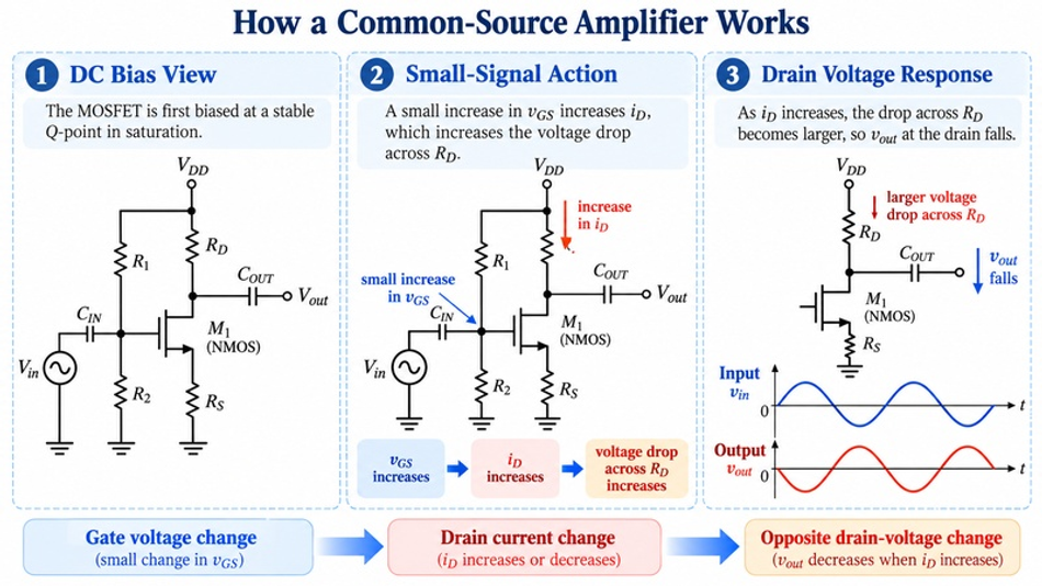
The DC bias network establishes the MOSFET operating point, while the AC input signal produces small changes in gate-to-source voltage V(GS). These changes alter the drain current ID. The changing drain current then produces a changing voltage drop across R(D), creating an amplified output voltage at the drain.
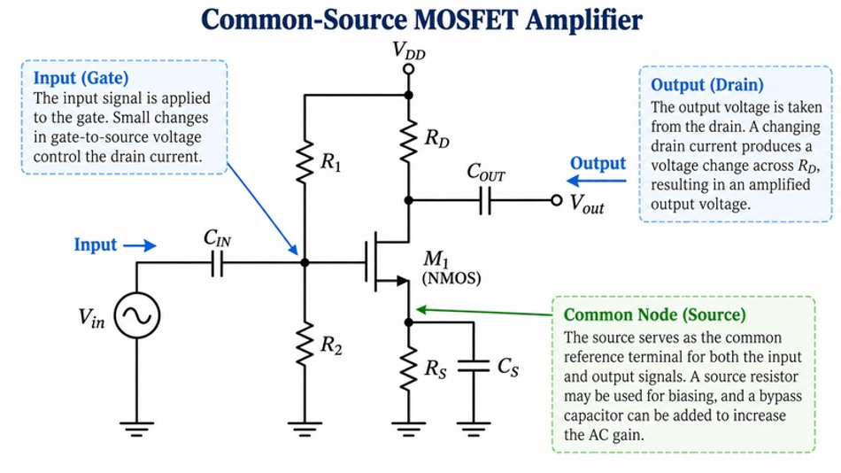
The word common means that the source terminal serves as the common reference node between the input and output portions of the stage. It does not necessarily mean that the physical source pin is directly connected to ground. A source resistor may be present while the source still functions as the common terminal from the amplifier-topology perspective. A common-source MOSFET amplifier is therefore primarily a voltage-amplification stage, unlike a common-drain stage, which is normally used when voltage buffering is more important than voltage gain.
How Does a Common-Source Amplifier Work?
A common-source amplifier operates in two stages. First, a small change in the gate-to-source voltage causes a change in the MOSFET drain current. Second, this change in drain current alters the voltage drop across the drain load, causing the drain voltage to move in the opposite direction. The MOSFET is first biased at a stable DC operating point, and the AC input is then applied as a small signal superimposed on that bias. This two-step process is the basis of MOSFET amplification in a MOSFET CS amplifier, producing both voltage gain and phase inversion.
DC Bias Point and Saturation-Region Operation
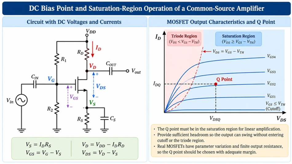
Before an AC signal can be amplified properly, the MOSFET must first be established at a suitable DC operating point, or Q point. In an NMOS common-source amplifier, the DC voltages at the gate, source, and drain determine the quiescent drain current and the available voltage range for the output signal to swing without excessive distortion.
The important DC quantities are:
V(G), V(S), V(GS), I(D), V(D), V(DS)
For a source resistor:
V(S) = I(D)R(S)
And:
V(GS) = V(G) − V(S)
The drain voltage is:
V(D) = V(DD) − I(D)R(D)
While:
V(DS) = V(D) − V(S)
For the simplified long-channel MOSFET model, saturation requires approximately:
V(DS) ≥ V(GS) − V(TH)
Or:
V(DS) ≥ V(OV)
Where:
V(OV) = V(GS) − V(TH)
is the overdrive voltage.
The threshold voltage V(TH) should not be treated as the gate-to-source voltage required for a desired amplifier bias current. It indicates the onset of channel conduction under specified conditions, not the correct operating point for linear amplification. A practical NMOS amplifier circuit should therefore establish its bias using device transfer characteristics, an appropriate MOSFET model, measurement, or another suitable bias method.
The saturation condition above is useful for understanding the circuit, but real MOSFETs also exhibit parameter variation, finite output resistance, and temperature dependence. The Q point must therefore provide sufficient headroom for the drain voltage to swing in both directions without entering cutoff or leaving the intended operating region. For additional background on gate-to-source voltage and drain-current control, see how a MOSFET works.
Small-Signal Amplification and 180∘ Phase Inversion
Suppose the input voltage of the common-source MOSFET amplifier rises slightly. This produces a small increase in the gate-to-source voltage v(gs), which in turn causes the drain current to increase. For sufficiently small signal variations around the Q point,
id=g(m)v(gs)
where g(m) is the MOSFET small-signal transconductance. It describes how effectively a small change in gate-to-source voltage produces a change in drain current. In this sense, the MOSFET acts as a transconductance device, converting a small input-voltage change into a corresponding change in drain current.
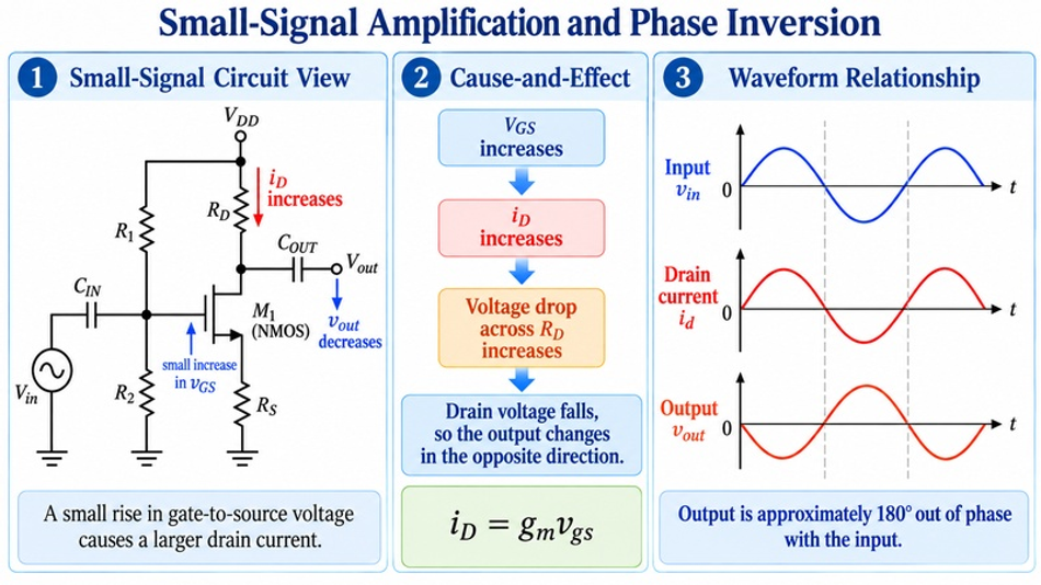
The increased drain current produces a larger voltage drop across the drain resistor R(D). Because the drain supply voltage V(DD) is fixed, a larger voltage drop across R(D) causes the drain voltage to fall. The opposite happens when the input voltage decreases: the drain current falls, the voltage drop across R(D) becomes smaller, and the drain voltage rises.
Therefore,
When the input voltage rises, the output voltage falls
When the input voltage falls, the output voltage rises
The output is therefore approximately 180∘ out of phase with the input. This phase inversion is a defining feature of MOSFET amplification in a common-source stage and explains the negative sign that appears later in the voltage-gain equation.
Common-Source Amplifier Gain and Impedance
The midband small-signal gain of a common-source amplifier depends on more than the MOSFET transconductance g(m) and drain resistor R(D). In a practical circuit, the external load, the MOSFET output resistance r(o), source degeneration, and the actual operating point can all change the measured gain. The input and output impedances also determine how strongly the amplifier interacts with the signal source and the following stage. For this reason, the gain is best developed step by step, beginning with the simplified case and then including the practical loading and feedback effects that influence real circuit behavior.
Calculating the Voltage Gain
For an idealized common-source stage operating at midband, assume that the MOSFET is biased in saturation, the input signal is small, the source is at AC ground, and the MOSFET output resistance r(o) is large enough to neglect. Under these conditions, the voltage gain is approximately
Av ≈ −gmR(D)
If an external load R(L) is connected to the output, it appears in parallel with R(D). Neglecting r(o), the gain becomes:
Av ≈ −gm(R(D) ∥ R(L))
This shows why a lower load resistance reduces the available voltage gain.
For a more practical small-signal model, the MOSFET's finite output resistance r(o) can also be included:
Av ≈ −gm(R(D) ∥ R(L) ∥ r(o))
Define the effective drain resistance as:
R(D,eff) = R(D) ∥ R(L) ∥ r(o)
Then:
Av ≈ −gmR(D,eff)
The negative sign represents the 180° phase inversion.
For example, suppose:
gm = 4 mSR(D) = 5.1 kΩR(L) = 47 kΩ
And:
r(o) = 100 kΩ
The effective drain resistance is approximately:
R(D,eff) = 5.1 kΩ ∥ 47 kΩ ∥ 100 kΩR(D,eff) ≈ 4.4 kΩ
Therefore:
Av ≈ −(0.004)(4400)Av ≈ −17.6
Under these assumptions, the stage has a midband voltage gain of approximately −17.6. In other words, a sufficiently small input change produces an output change about 17.6 times larger and of opposite polarity.
The value of g(m) should be determined at the actual operating point using an appropriate device model, simulation, measurement, or suitable datasheet information. It should not be treated as a fixed value that applies to the MOSFET under all bias conditions.
How Source Degeneration Changes Gain and Linearity
An unbypassed source resistor R(S) introduces local negative feedback, often called source degeneration. When the drain current increases, the voltage across R(S) also increases:
V(S)=I(D)R(S)
Because
V(GS)=V(G)−V(S)
the resulting rise in source voltage reduces the change in V(GS) that originally caused the drain current to increase. This feedback lowers the voltage gain, but it also makes the amplifier less sensitive to variations in MOSFET parameters and generally improves linearity.
At midband, for small signals, with the MOSFET biased in saturation and r(o) assumed large enough to neglect, the voltage gain can be approximated as
A(v) ≈ -g(m)R(D,eff) / 1+g(m)R(s)
Using the earlier example
(m)=4mS, R(D)=5.1kΩ, R(L)=47kΩ
and
R(s)=1.5kΩ
gives
g(m)R(s)=(0.004)(1500)=6
and therefore
A(v) ≈ -17.6A(v) / 1+6 ≈ -2.51
| Characteristic | Unbypassed R(S) | R(S) bypassed by C(S) |
| AC negative feedback | Strong | Reduced at frequencies where C(S) has low impedance |
| Voltage gain | Lower | Higher |
| Linearity | Better | Usually lower than unbypassed case |
| Gain sensitivity to device variation | Lower | Higher |
| DC bias stabilization | Retained | Retained |
| Frequency dependence | Limited | Depends on C(S) |
So, source degeneration lowers the voltage gain substantially, but it can improve bias stability, gain predictability, linearity, and useful output-swing behavior. If R(S) is bypassed by a capacitor that presents sufficiently low impedance at the signal frequency, much of the AC feedback is reduced and the voltage gain increases. The bypass capacitor therefore allows the circuit to retain the DC bias-stabilizing effect of R(S) while recovering more AC gain over the frequency range in which the capacitor is effective.
Input and Output Impedance
The MOSFET gate draws very little low-frequency input current, but this does not mean that the practical input impedance is infinite. In a common-source amplifier, the input impedance seen by the signal source is mainly determined by the gate-bias network.
For a divider formed by R(1) and R(2)
Z(in) ≈ R(1) ∥ R(2)
This bias-network combination can be viewed as the effective gate resistance presented to the signal source at low frequencies.
The unloaded output impedance is approximately:
Z(out) ≈ R(D) ∥ r(o)
If a load impedance R(L) is connected, the drain experiences:
R(D) ∥ r(o) ∥ R(L)
A relatively low load impedance R(L) therefore decreases the effective drain resistance and reduces the available voltage gain.
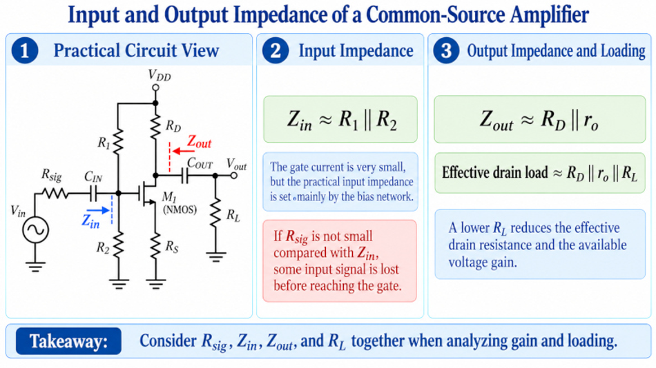
Considering these quantities together is important for practical impedance matching and for preventing excessive signal loss between amplifier stages. If the source resistance is not small compared with the amplifier input impedance, part of the input signal is lost before it reaches the MOSFET gate. Similarly, the following-stage load becomes part of the effective drain resistance and can reduce the voltage gain. In practical design, R(in), source resistance, R(out), and R(L) should therefore be considered together rather than treating the amplifier as an isolated stage.
How to Draw and Calculate a Practical NMOS Amplifier Circuit
Consider a single-supply, enhancement-mode NMOS amplifier circuit with a resistive drain load and voltage-divider bias. The circuit includes:
Supply voltage V(DD)
Gate-bias resistors R(1) and R(2)
Drain resistor R(D)
Source resistor R(S)
Input capacitor C(IN)
Output capacitor C(OUT)
Optional source-bypass capacitor C(S)
To draw and calculate a practical MOSFET amplifier circuit, first define the required operating point, expected input signal, load, gain, and frequency range. These requirements are then used to determine the resistor and capacitor values. Selecting convenient component values before defining the Q point can lead to poor voltage headroom, incorrect bias current, or unnecessary signal distortion.
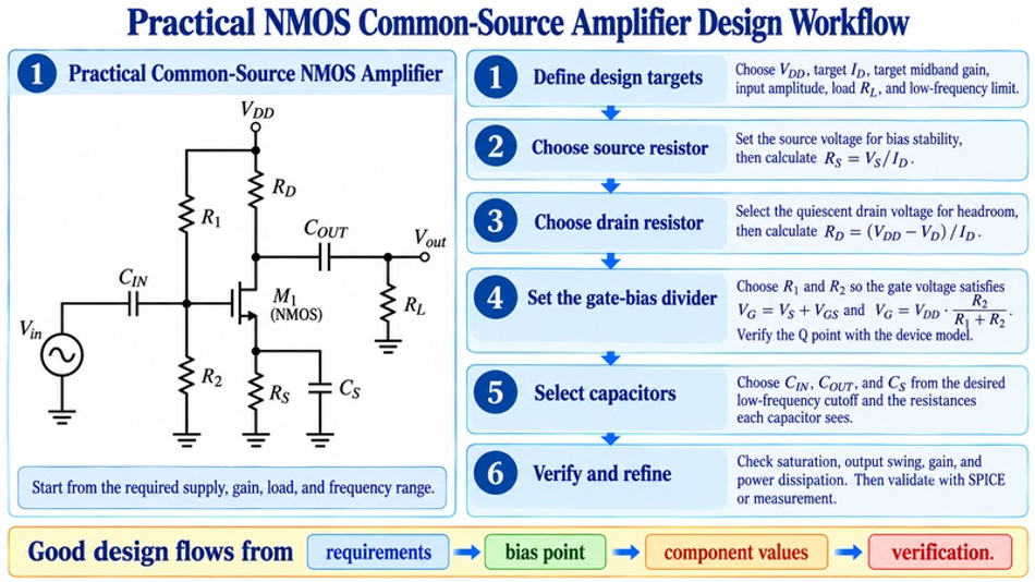
Define the Design Requirements and Draw the Circuit
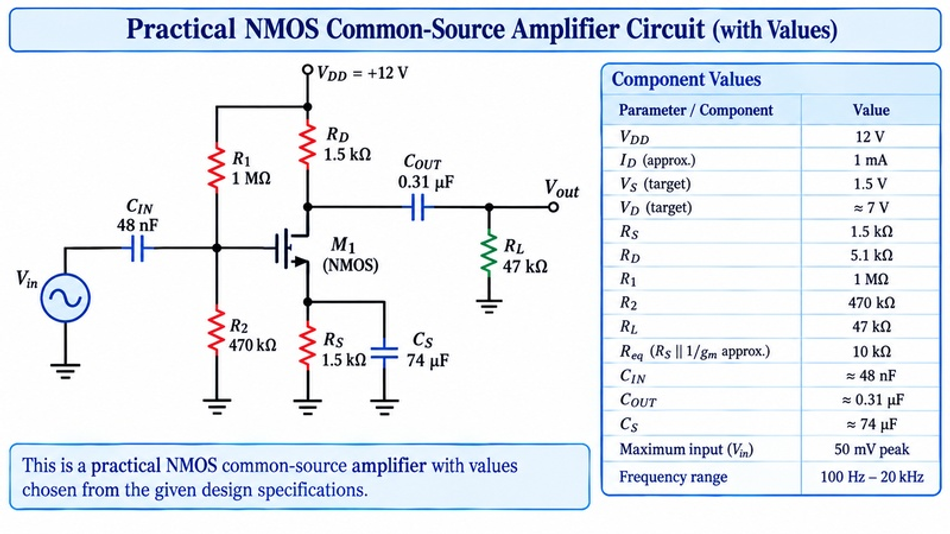
For this teaching example, use the following design targets. These values are illustrative rather than universal recommendations:
| Design parameter | Teaching target |
| V(DD) | 12 V |
| I(D)Voltage gain | 1 mA |
| V(S)Linearity | 1.5 V |
| V(D) | ≈7 V |
| R(L) | 47 kΩ |
| R(sig) | 10 kΩ |
| Maximum input | 50 mV peak |
| Frequency range | 100 Hz–20 kHz |
| Target bypassed midband gain | approximately −15 to −18 V/V |
Calculate the Bias Network, Drain Resistor, and Source Resistor
Start with the source resistor:
R(S)=V(S)/I(D)
R(S)=1.5/0/001
R(S)=1.5 kΩ
Next calculate the drain resistor:
R(D)=[V(DD)-V(D)] / I(D)
R(D)=(12-7)/0.001
R(D)=5 kΩ
A nearby standard value is
R(D)=5.1 kΩ
At I(D)= 1mA,
V(D)=12−(0.001)(5100)
V(D)=6.9 V
The resulting drain-to-source voltage is
V(DS)=V(D)-V(S)
V(DS)=6.9-1.5
V(DS)=5.4V
This provides substantial voltage headroom for a typical small-signal operating point.
The gate voltage can be generated using a divider:
V(G)=V(DD) [R(2)/(R(1)+R(2)]
For example, choose
R(1)=1 MΩ
and
R(2)=470 kΩ
Then
V(G)=12 [470 kΩ/(1 MΩ+470 kΩ]
V(G)≈3.84V
This divider establishes a nominal gate voltage of approximately 3.84V. However, this value alone does not guarantee I(D) = 1 mA, because the relationship between V(GS) and drain current depends on the selected MOSFET and its actual operating characteristics.
The corresponding bias-network input impedance is approximately
R(in) ≈ 1MΩ ∥ 470kΩ
R(in) ≈ 320kΩ
Because MOSFET characteristics vary from device to device, the final I(D) should be verified using an appropriate SPICE simulation, transfer characteristics, measurement, or a more stable bias arrangement when greater accuracy is required. Once these design requirements are established, you can browse MOSFETs for amplifier designs and compare suitable devices against the required operating conditions.
Select the Coupling and Bypass Capacitors
The input and output coupling capacitors block DC while allowing the AC voltage component of the signal to pass. Together with the resistance, they create high-pass networks.
For a simple first-order high-pass network,
f(c) = 1 / (2πR(eq)C)
For the input capacitor,
C(IN) ≈ 1 / (2πf(c,in)R(eq,in))
where R(eq,in) includes the relevant source resistance and amplifier input impedance.
R(eq,in) ≈ R(sig) + R(in)
R(eq,in) ≈ 10k + 320k = 320 kΩ
Choose an individual coupling pole around 10 Hz, below the desired 100 Hz operating band:
C(IN) ≈ 1 / (2π(10)(330k))
C(IN) ≈ 48 nF
For the output,
C(OUT) ≈ 1 / (2πf(c,out)R(eq,out))
Using:
R(out) ≈ R(D) ∥ r(o)
With the earlier example:
R(out) ≈ 5.1k ∥ 100k ≈ 4.85kΩ
Then:
R(eq,out) ≈ R(out) + R(L)
R(eq,out) ≈ 4.85k + 47k ≈ 51.9kΩ
And:
C(OUT) ≈ 1 / (2π(10)(51.9k)) ≈ 0.31 μF
For the bypass capacitor, using the simplified midband approximation:
R(source,eq) ≈ R(S) ∥ (1/g(m))
With:
R(S) = 1.5kΩ
1/g(m) = 250Ω
R(source,eq) ≈ 214Ω
So approximately:
C(S) ≈ 1 / (2π(10)(214)) ≈ 74 μF
The capacitor values should be chosen from the desired low-frequency cutoff and the impedances surrounding each capacitor. Once the required values are known, browse coupling and bypass capacitors and compare capacitance, voltage rating, tolerance, dielectric type, and package size.
Verify Saturation, Output Swing, Gain, and Power Dissipation
The calculated component values should now be checked to confirm that the amplifier can operate as intended. At the estimated Q point,
V(D) ≈ 6.9V
And:
V(S) ≈ 1.5V
Giving:
V(DS) ≈ 5.4V
The design should now be checked against the MOSFET model to confirm adequate saturation margin.
For upward drain swing, the theoretical supply limit is approximately:
12 − 6.9 = 5.1V
For downward swing, the drain must remain high enough above the source to satisfy the required operating-region condition. The actual permissible amplitude is therefore determined by whichever limit is reached first. Resistor dissipation should also be checked. For the drain resistor,
The power dissipated by the drain resistor is:
P(RD) = I(D)²R(D)
P(RD) = (0.001)²(5100)
P(RD) = 5.1mW
For the MOSFET:
P(D) ≈ V(DS)I(D)
P(D) ≈ (5.4)(0.001)
P(D) ≈ 5.4mW
With g(m) = 4mS, R(D) = 5.1kΩ, R(L) = 47kΩ, and r(o) = 100kΩ, the earlier small-signal calculation gives a bypassed midband gain of approximately −17.6V/V. For a 50mV peak input, the corresponding ideal small-signal output amplitude is approximately:
|V(o)| ≈ 17.6(50mV)
|V(o)| ≈ 0.88V peak
This is well below the approximately 5.1V upward supply-side headroom calculated from the Q point. The lower swing limit must still be checked using the selected MOSFET model because the required saturation margin depends on its actual operating characteristics.
| Parameter | Result |
| V(D) | ≈6.9 V |
| V(S) | ≈1.5 V |
| V(DS) | ≈5.4 V |
| Calculated bypassed gain | ≈−17.6 V/V |
| Input example | 50 mV peak |
| Expected output | ≈0.88 V peak |
| Upward drain headroom | ≈5.1 V |
| Downward saturation margin | Verify with chosen MOSFET model |
| P(RD) | ≈5.1 mW |
| P(D) | ≈5.4 mW |
Common-Source vs. Common-Drain Amplifier
A common-source and a common-drain amplifier use the same basic transistor but serve different circuit purposes. This brief comparison is intended only to prevent topology confusion:
| Property | Common-Source | Common-Drain |
| Input terminal | Gate | Gate |
| Output terminal | Drain | Source |
| Common terminal | Source | Drain |
| Voltage phase | Inverted | Non-inverted |
| Typical voltage gain | Can be greater than 1 | Usually below 1 |
| Input impedance | High | High |
| Output impedance | Moderate | Relatively low |
| Common use | Voltage amplification | Buffering / impedance transformation |
The common-source stage is normally chosen when substantial voltage amplification is required. A common-drain amplifier, also called a source follower, is more suitable when the objective is to buffer a high-impedance source and drive a lower-impedance load. For a more detailed explanation of the buffering topology, see our voltage follower guide.
Simulate and Test the Amplifier
A practical MOSFET amplifier circuit should be validated at three levels:
Hand calculation establishes expected values
Simulation checks the transistor model and loading effects
Measurement confirms actual hardware behavior.
These three steps complement one another. Calculations provide the starting point, simulation tests the design model, and measurement verifies the real circuit.
Compare Hand Calculations with SPICE Results
Begin with a DC operating-point analysis. Check
I(D), V(G), V(S), V(D), V(GS), V(DS)
against the calculated Q point.
Next, run an AC analysis and measure the midband voltage gain:
A(v) = V(o)/ V(i)
Finally, perform a transient simulation with a sinusoidal input. Confirm that the output is inverted and remains undistorted over the required signal amplitude.
| Quantity | Hand calculation | SPICE result | Difference |
| I(D) | ... | … | … |
| V(G) | … | … | … |
| V(D) | … | … | … |
| V(DS) | … | … | … |
| Midband gain | … | … | … |
| Lower cutoff | … | … | … |
| Maximum clean output swing | … | … | … |
Differences between hand calculations and simulation are normal because a practical SPICE model includes effects that the simplified analysis may ignore, particularly finite output resistance, nonlinear transconductance, and device capacitance and the Miller effect.
Diagnose Low Gain, Clipping, and Bias Errors
If measured or simulated performance differs from the calculation, check the symptoms systematically.
| Symptoms | Possible cause | First check |
| Gain lower than expected | Load resistance too low | Measure effective drain load |
| Gain lower than expected | g(m) lower than assumed | Check actual Q point |
| Large DC output shift | Incorrect bias point | Measure V(G), V(S), V(D) |
| Positive-side clipping | Insufficient supply headroom | Check drain Q-point voltage |
| Negative-side clipping | MOSFET leaving intended region | Check V(DS) during signal swing |
| Distorted waveform | Input signal too large | Reduce input amplitude |
| Gain changes between devices | MOSFET parameter variation | Compare transfer characteristics |
| Unexpected low-frequency loss | Coupling/bypass capacitors too small | Check capacitor corner frequencies |
If the measured gain is smaller than
-g(m)R(D)
that does not automatically mean the equation has failed. The simplified equation may be ignoring RL, ro, source degeneration, device variation, or another relevant loading effect.
How to Choose a MOSFET for a Common-Source Amplifier
MOSFET selection should take place after the required bias current, voltage swing, gain, and loading have been established. For a small-signal common-source amplifier, a low value of R(DS)(on) is not usually the primary selection criterion. R(DS)(on) is especially important in switching and power electronics applications, whereas amplifier design depends strongly on operation around the chosen Q point.
Useful datasheet and model parameters include:
| Parameter | Why it matters | What to verify |
| V(D) rating | Device must withstand circuit voltage | Rating exceeds expected maximum |
| I(D) rating | Device must safely carry bias and signal current | Adequate current margin |
| Transfer characteristics | Helps estimate the required V(GS) | Desired I(D) is achievable |
| g(m) | Strongly affects voltage gain | Value near intended Q point |
| V(TH) range | Shows device variation | Do not treat it as the required bias voltage |
| r(o) or output characteristics | Affects effective gain | Check drain-current dependence on V(DS) |
| Input and feedback capacitances | Affect higher-frequency behavior | Appropriate for intended bandwidth |
| Noise data | Important for low-level signals | Check when low noise is required |
| Package / thermal data | Determines allowable dissipation | Verify junction temperature |
| SPICE model | Improves simulation accuracy | Prefer an appropriate manufacturer model |
The key question is not simply whether the MOSFET can turn on. It is whether its characteristics are suitable at the intended I(D), V(DS), V(GS), signal amplitude, and frequency range.
Once these requirements are known, you can browse the Unikeyic MOSFET product catalog and compare candidate devices by voltage, current, transconductance, capacitance, thermal limits, package, and available SPICE models.
Frequently Asked Questions
The following frequently asked questions address common points about common-source MOSFET amplifiers, including their operation, voltage gain, phase inversion, biasing, and practical design considerations. They are intended to clarify key concepts and help readers better understand how common-source amplifier circuits behave in typical applications.
1. What does “common” mean in a common-source amplifier?
“Common” means that the source terminal acts as the reference terminal shared by the input and output signal paths. The signal enters through the gate and leaves through the drain, while the source is common to both sides of the amplifier.
2. Why does a common-source amplifier invert the signal?
An increase in V(GS) increases I(D). The larger drain current creates a greater voltage drop across R(D), causing the drain voltage to fall. Therefore, the output changes in the opposite direction to the input, producing an approximately 180° phase inversion.
3. What is the difference between a common-source and common-drain amplifier?
A common-source amplifier is primarily used for voltage gain and produces an inverted output. A common-drain, or source-follower, stage usually has a voltage gain below unity but offers lower output impedance, making it useful as a buffer.
4. Must the MOSFET operate in saturation to amplify?
For the conventional small-signal common-source amplifier discussed here, the transistor is normally biased in its saturation region. This allows drain current to be controlled mainly by changes in V(GS) around the Q point and provides useful voltage gain.
5. Why is measured gain lower than −g(m)R(D)?
Measured gain is often lower than A(v) ≈ −g(m)R(D) because that equation assumes an idealized common-source stage. In a real circuit, the external load R(L), MOSFET output resistance r(o), source degeneration through R(S), and the actual value of g(m) all affect gain.
A more practical expression:
A(v) ≈ −g(m)(R(D) ∥ R(L) ∥ r(o))
includes these loading and feedback effects, so the measured voltage gain is usually smaller than the ideal value.
6. Can any NMOS be used in a common-source amplifier?
Many enhancement-mode NMOS devices can operate in a common-source topology, but that does not make every device suitable for every design. The intended drain current, g(m), required bias voltage, capacitances, noise, output characteristics, package, dissipation, and available device model should all be considered.
Conclusion
Overall, a common-source amplifier converts small changes in MOSFET gate-to-source voltage into larger, inverted voltage changes at the drain. Successful design begins by establishing a suitable Q point, ensuring saturation-region operation, calculating the drain and source resistors, and then determining gain using the actual effective load rather than relying only on the ideal expression −g(m)R(D).
The completed circuit should then be checked for input and output impedance, coupling-capacitor behavior, output swing, clipping, device variation, and output power dissipation before being verified with SPICE simulation and measurement.
With the electrical requirements established, the final step is to find a MOSFET for your amplifier circuit by comparing appropriate MOSFET datasheet parameters and device models rather than selecting a device from switching specifications alone.