What Is a Junction Field-Effect Transistor (JFET)? Types, Operation, and Selection
A JFET is a normally-on, voltage-controlled semiconductor device that regulates current through a conductive channel by varying its depletion region using an electric field.

16 Nov, 2026. 13 minutes read
This article was first published on
www.unikeyic.comA junction field-effect transistor (JFET) is a three-terminal, voltage-controlled semiconductor device. It controls current through a conductive channel using an electric field. A JFET is a unipolar device, so current is carried mainly by one type of majority carrier. In contrast, a bipolar junction transistor (BJT) relies on both electrons and holes. The JFET gate forms a PN junction with the channel, and this junction is normally reverse biased. The gate-to-source voltage controls the width of the depletion region around this junction. As the depletion region expands or contracts, the effective channel width changes. This directly affects the drain current. Most conventional JFETs are normally on, which means a conductive path already exists when the gate-to-source voltage is zero ( V(GS)=0 ).
What Is a Junction Field-Effect Transistor?
JFET stands for Junction Field-Effect Transistor. It belongs to the wider field-effect transistor family, but its control mechanism differs from that of a MOSFET. Instead of using an insulated oxide gate, a junction field-effect transistor uses a PN junction between the gate region and semiconductor channel. This junction creates a depletion region containing few mobile charge carriers. By changing the reverse bias applied between Gate and Source, the depletion layers can be widened or narrowed. That, in turn, changes the usable cross-sectional area of the channel and controls current flowing between Drain and Source.
JFET Structure, Terminals, and Circuit Symbol
A basic junction field-effect transistor has three terminals:
| Terminal | Function |
| Gate (G) | Controls channel conductivity through the gate-channel PN junction |
| Source (S) | Terminal from which majority carriers enter the channel in normal operation |
| Drain (D) | Terminal toward which majority carriers travel in normal operation |
In an N-channel JFET, the main channel is N-type semiconductor, and the gate regions are P-type. Electrons are therefore the majority charge carriers. In a P-channel JFET, the materials are reversed and holes are the majority carriers.
The JFET transistor diagram and circuit symbols below help distinguish between the two channel types. In the junction field effect transistor symbol, the gate arrow identifies the PN-junction orientation and points toward N-type material. Consequently, the arrow points toward the channel for an N-channel JFET and away from the channel for a P-channel device. However, symbol conventions can vary, so always check the device datasheet to confirm the channel type and pinout.”
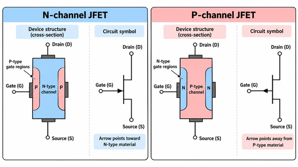
Although Source and Drain may appear structurally similar in some JFETs, designers should not assume that they are interchangeable in every device or circuit. Internal geometry, electrical characteristics, package pin assignments, and manufacturer specifications can distinguish between the two terminals. The device datasheet should therefore be the final reference.
Why a JFET Is Normally On and Voltage Controlled
A conventional JFET already contains a physical conducting channel when no gate-to-source bias is applied. When a drain-to-source voltage V(DS) is applied while V(GS) = 0, drain current can flow through this existing channel. For this reason, a conventional JFET is described as a normally-on device.
In an N-channel JFET, a gate voltage that becomes increasingly negative relative to the source places the gate-channel PN junction under stronger reverse bias. The depletion layers then extend farther into the N-type channel. As the conductive path becomes narrower, its effective resistance increases and the drain current decreases. The same basic control principle applies to a P-channel JFET, but the normal voltage polarities are reversed.
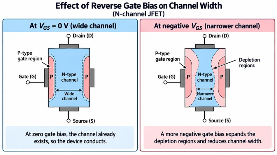
The gate-channel junction remains reverse biased during normal operation, so the steady-state gate current is usually very small compared with the channel current. This behavior gives JFETs a high input impedance and allows the gate voltage to control channel current without requiring substantial continuous gate current.
This normally-on behavior distinguishes JFET transistors from common enhancement-mode MOSFETs, which are typically normally off and require gate bias to establish a conductive channel.
How Does a JFET Work?
Consider an N-channel JFET. Two voltages play different roles. The drain-source voltage V(DS) establishes the electric potential difference along the channel and drives current between the source and drain, while the gate-source voltage V(GS) controls the channel’s effective width.
This distinction is important. The gate does not normally control drain current by continuously injecting charge carriers into the channel. Instead, the electric field associated with the reverse-biased gate junction changes the depletion regions and, in turn, the effective geometry of the conductive channel.
Reverse Gate Bias and Depletion-Region Control
At V(GS) = 0, the channel is at its most conductive normal gate-bias condition. As V(DS) is applied, electrons in an N-channel JFET move through the channel while conventional drain current is defined in the opposite direction.
When the Gate becomes negative relative to the Source, the gate-channel PN junction becomes more strongly reverse biased. Its depletion region expands. Because this region has few mobile carriers, the effective width of the conductive N-type channel decreases.
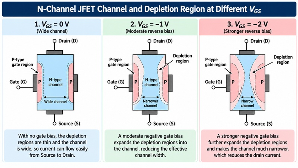
Increasing the reverse bias further produces a narrower channel, greater effective channel resistance, and lower drain current. Eventually a sufficiently reverse V(GS) can reduce I(D) to a very small value. The P-channel device operates according to the same physical mechanism, but carrier type and normal voltage polarities are reversed.
Pinch-Off Is Not the Same as Cutoff
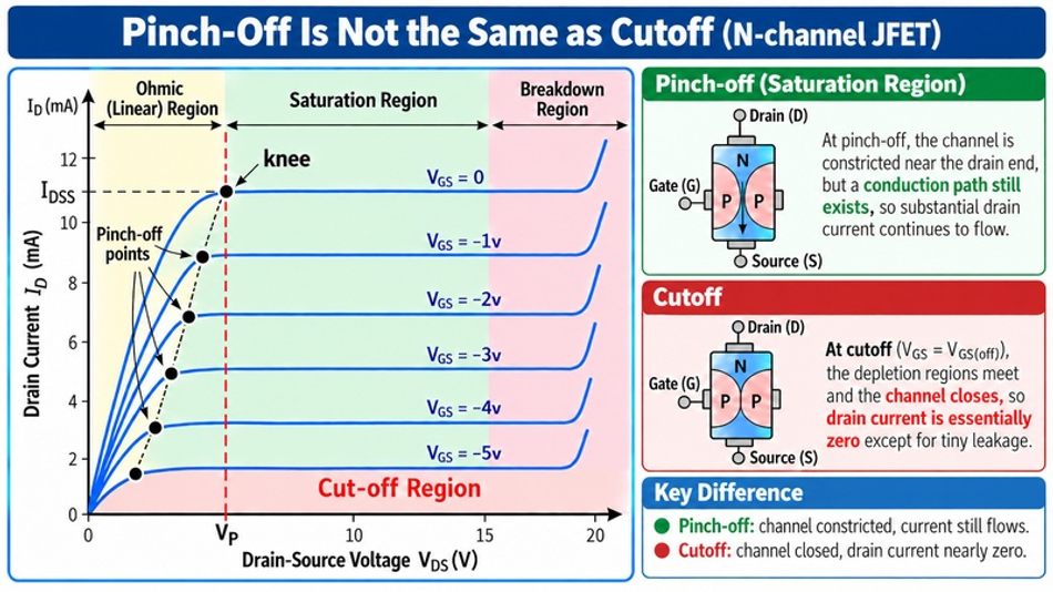
Pinch-off and cutoff should not be treated as synonyms. As V(DS) increases in an operating JFET, the gate-to-channel reverse bias is not identical at every point along the channel. The depletion region becomes wider toward the Drain. At a sufficient V(DS), the channel becomes strongly constricted near the drain end. At this point, the pinch-off condition is reached, and the JFET enters the saturation region.
The important point is that drain current does not become zero at this event. Once V(DS) increase and reaches the pinch-off condition, the device continues to conduct, and I(D) becomes comparatively insensitive to further increases in V(DS), although the current in a real Junction FET is not perfectly constant.
By contrast, cutoff is reached when the gate-to-source reverse bias is sufficient to reduce drain current to the small value used by the manufacturer to define V(GS(off)).
N-Channel vs. P-Channel JFET
An N-channel JFET and P-channel JFET use the same fundamental field-control mechanism. Their main differences are the semiconductor type forming the channel, the majority carriers, normal voltage polarities, conventional-current direction, and circuit-symbol arrow.
| Characteristic | N-channel JFET | P-channel JFET |
| Majority carriers | Electrons | Holes |
| Channel material | N-type | P-type |
| Gate material | P-type | N-type |
| Typical V(GS) control | Zero to negative | Zero to positive |
| Typical Drain polarity | Positive relative to Source | Negative relative to Source |
| Symbol arrow | Toward channel | Away from channel |
N-Channel JFET
An N-channel JFET uses an N-type semiconductor channel, so electrons are the majority charge carriers. During normal operation, the drain is usually positive relative to the source, while the gate is held at the same potential as the source or at a negative voltage relative to it.
A more negative V(GS) increases the reverse bias across the gate-channel PN junction. The depletion region then extends farther into the N-type channel, reducing its effective width and lowering the drain current. At V(GS) = 0, the channel remains conductive, which is why a conventional N-channel JFET is normally on.
The exact allowable values of V(GS), V(DS), drain current, and power dissipation depend on the individual device. Designers should therefore check the manufacturer datasheet rather than applying generic JFET values to a specific circuit.
P-Channel JFET
A P-channel JFET uses holes as the majority charge carriers. Compared with an N-channel JFET, the usual voltage polarities and conventional-current direction are reversed. The drain is normally negative relative to the source, while a positive gate voltage relative to the source provides the reverse bias required for channel control.
The operating principle remains the same. A stronger reverse gate bias widens the depletion region, reduces the effective channel width, and lowers the drain current. The polarity of these voltages, however, is opposite to that used with an N-channel device.
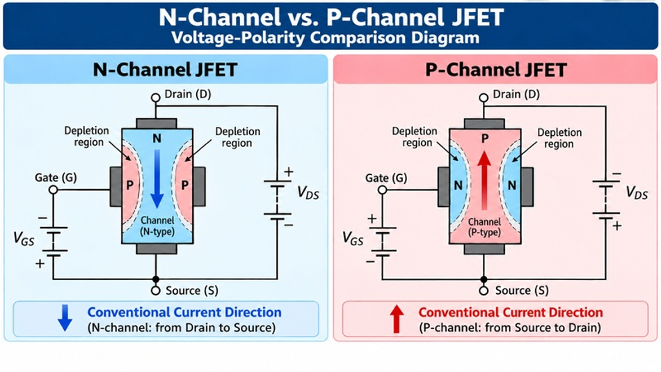
Engineers should not directly apply N-channel voltage signs or parameter conventions to a P-channel circuit. The manufacturer datasheet should be checked for symbol definitions, polarity conventions, test conditions, and allowable voltage and current limits.
After identifying the required channel polarity, engineers can browse N-channel and P-channel JFETs and compare candidate devices using their datasheets and circuit requirements.
JFET Operating Regions and Characteristic Curves
After comparing N-channel and P-channel devices, the next step is to see how JFET characteristics are represented on datasheet curves. Two plots are particularly useful. The output characteristics show how drain current I(D) changes with drain-source voltage V(DS) at different values of gate-source voltage V(GS), helping identify the device’s operating region. The transfer characteristic shows how I(D) varies with V(GS) under specified conditions. In simple terms, the output curves show how the JFET behaves across its operating regions, while the transfer curve shows how gate voltage controls drain current.
Ohmic, Saturation, Cutoff, and Breakdown Regions
At low V(DS), a JFET operates in its ohmic or linear region. The channel behaves approximately like a voltage-controlled resistance, making this region relevant to some variable-resistance and switching applications.
As V(DS) increase and reaches the pinch-off condition, the JFET enters the saturation region. Drain current is then controlled primarily by V(GS) and changes less dramatically with V(DS). Amplifier circuits normally establish their operating point in this general region.
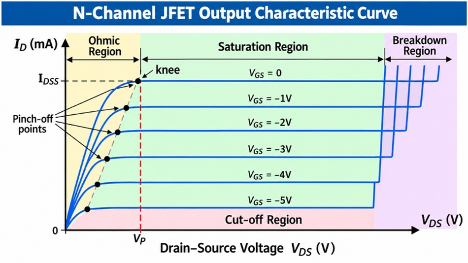
In cutoff, sufficiently strong reverse Gate bias has reduced I(D) to approximately the datasheet-defined off-state level.
The breakdown region occurs when device voltage ratings are exceeded sufficiently for breakdown mechanisms to produce a rapid current increase. It is normally outside the intended operating region and should not be treated as another useful bias mode.
Real datasheet curves illustrate that saturation-region current is not an ideal horizontal line. As one device-specific example, onsemi 2N5457/2N5458 datasheet characteristics show I(D) versus V(DS) curves changing with both V(GS) and operating conditions. These curves are specific to the corresponding part numbers and should not be treated as universal JFET characteristics.
Understanding I D S S , V G S ( o f f ) , and Transconductance
Three parameters appear frequently when evaluating JFET transistors:
| Parameter | What it tells you | What must be checked |
| I(DSS) | Drain current at V(GS) = 0 under specified conditions | V(DS), temperature, min/max range and test conditions |
| V(GS(off)) | Gate-source voltage at which I(D) falls to a specified small value | Defined test current, V(DS), sign convention and range |
| g(m) or g(fs) | Small-signal change in Drain current for a change in Gate voltage | Operating current, V(DS), frequency and test conditions |
I(DSS) indicates the drain current measured with zero gate-to-source bias, but it is not a universal current value for every operating condition. The stated V(DS), temperature, and datasheet limits must also be considered. V(GS(off)) indicates the gate-source voltage at which drain current has fallen to the small value defined by the manufacturer. Its sign and test current are important because datasheets do not always use identical conventions.
Transconductance describes how strongly drain current responds to a small change in gate voltage around a particular operating point. Because it depends on bias current and other test conditions, it should not be treated as a fixed value for the device.
As one device-specific example, the onsemi 2SK545 datasheet specifies I(DSS) at V(DS) = 10 V and V(GS) = 0, while V(GS(off)) is specified using a different drain-current condition. Forward-transfer admittance is also given under its own voltage and frequency conditions. These parameter values and test conditions apply specifically to the 2SK545 and should not be assumed to represent all JFETs.
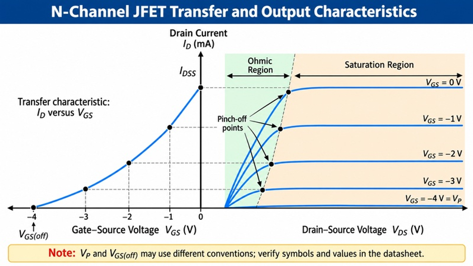
These values can vary significantly even between devices with the same part number. For that reason, engineers should check minimum and maximum limits rather than relying only on typical values. Also check notation carefully. Datasheets and textbooks do not always use V(P), pinch-off, and V(GS(off)) in the same way or with the same sign convention.
JFET vs. MOSFET vs. BJT
The search phrase “JFET vs transistor” is technically imprecise because JFETs, MOSFETs, and BJTs are all transistors. A useful comparison instead looks at their control mechanisms and application characteristics.
| Characteristic | JFET | MOSFET | BJT |
| Control | Gate voltage | Gate voltage | Base current / base-emitter drive |
| Input structure | Reverse-biased PN junction | Insulated gate | Forward-biased base-emitter junction during normal conduction |
| Default state | Usually normally on | Enhancement types usually normally off | Normally off without base drive |
| Carrier type | Unipolar | Unipolar | Bipolar |
| Input current | Very small under reverse gate bias | Very small steady-state gate current | Requires base current |
| Input impedance | High | Very high | Lower |
| Important design strengths | High-impedance and selected low-noise analog work | Digital logic, switching, power conversion and extensive analog use | High transconductance and many analog/current-drive applications |
Toshiba’s comparison of BJTs and MOSFETs classifies MOSFETs as voltage-driven, high-input-impedance devices and BJTs as current-driven devices. Modern enhancement-mode MOSFETs are also normally off, distinguishing their default behavior from conventional JFETs.
There is no universal answer to whether a MOSFET is better than a JFET. The appropriate device depends on factors such as source impedance, biasing requirements, noise, transconductance, switching or linear operation, operating frequency, voltage and current requirements, capacitance, availability, and the overall circuit requirements.
JFET Advantages, Limitations, and Applications
JFETs are valuable in specific analog situations rather than as universal replacements for MOSFETs or BJTs. Their very low gate current and high input impedance can benefit high-source-impedance signals, while selected devices may also provide useful low-noise performance. These advantages are application-dependent: source impedance, operating frequency, bias current, parameter spread, capacitance, voltage limits, and package availability all affect whether a JFET is a good fit. The same device characteristic that helps one circuit may offer little benefit in another design.
Practical Advantages and Limitations
A reverse-biased gate junction allows a JFET to operate with very low gate current and high input impedance, which helps minimize loading on high-source-impedance signal sources. Selected JFETs can also provide useful low-noise performance, particularly in circuits with high source impedance. Analog Devices’ discrete-amplifier design article discusses discrete matched JFET input stages for high-input-impedance, low-noise instrumentation applications.
These advantages are application dependent. Noise performance varies with the specific device, source impedance, operating frequency, bias point, and surrounding circuit. A JFET is therefore not necessarily the choice for every signal source or operating condition.
Parameter spread is another practical issue. I(DSS) and V(GS(off)) can span significant ranges, so circuits that depend heavily on exact typical values may show poor unit-to-unit repeatability.
Engineers must also consider gate-junction forward-bias limits, voltage and power ratings, transconductance, gate leakage current, parasitic capacitances such as C(GS) and C(GD), temperature behavior, and package availability.
Where JFETs Are Still Used
JFETs are not obsolete. They remain useful in high-input-impedance sensor interfaces, low-noise analog front ends, audio and instrumentation inputs, selected RF circuits, analog switching, and current-regulation applications. Their high input impedance is particularly useful with devices such as photodiodes, piezoelectric sensors, and other high-impedance transducers, where input-current effects can become important.
For amplifier circuits, three familiar arrangements are the common-source, common-drain/source-follower, and common-gate configurations. Although JFET and MOSFET bias requirements differ, our practical common-source MOSFET amplifier guide provides a useful example of common-source gain, biasing, impedance, and signal-swing calculations.
MOSFET/CMOS technology dominates modern digital logic, but that does not eliminate the JFET's specialized role in analog circuitry.
How to Select a JFET Transistor
JFET selection should begin with the circuit requirement, not with a popular part number or a single attractive specification. First determine whether the JFET will be used for amplification, buffering, current regulation, variable resistance, switching, sensor interfacing, or another analog function. Then establish the required channel type, supply polarity, signal range, expected drain current, allowable voltage stress, operating temperature, bandwidth, and source impedance.
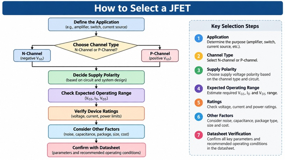
Start With the Application and Channel Type
For a conventional positive-supply common-source stage, an N-channel JFET may fit naturally. Another architecture or polarity requirement may point to a P-channel device.
Next establish the expected operating current and signal swing. A device whose I(DSS) range bears little relationship to the required operating point may complicate biasing even if its maximum voltage rating appears adequate.
For noise-sensitive designs, source impedance and frequency need to be considered together with the transistor's noise specifications rather than simply choosing whichever datasheet advertises the smallest noise number.
Check Electrical, Noise, Capacitance, and Package Parameters
After the architecture has narrowed the device class, verify the datasheet systematically.
| Parameter | Why it matters | Primary source |
| V(DS) rating | Voltage-survival margin | Absolute maximum ratings |
| I(D) rating | Current capability | Ratings and characteristics |
| I(DSS) | Zero-gate-bias current range | Electrical characteristics |
| V(GS(off)) | Gate-bias range required for cutoff | Electrical characteristics |
| g(m) / g(fs) | Gain and small-signal response | Characteristics/curves |
| Gate leakage | Loading of very high-impedance sources | Electrical characteristics |
| Noise | Front-end signal-to-noise performance | Noise curves/test conditions |
| C(GS), C(GD) | Frequency response and loading | Capacitance specifications |
| Power dissipation | Thermal operating limit | Maximum ratings |
| Temperature range | Environmental suitability | Ratings |
| Package / pinout | PCB, thermal and assembly compatibility | Package information |
The full minimum/maximum range and the associated test conditions matter more than an isolated typical number. A manufacturer datasheet should remain the design authority if a distributor description and datasheet disagree.
After defining the required channel type, voltage and current ranges, I(DSS), V(GS(off)), noise, capacitance, and package requirements, you can view Unikeyic’s JFET product catalog and compare candidate devices. Always verify the final choice against the manufacturer datasheet and the requirements of the specific circuit.
Frequently Asked Questions About JFETs
The following FAQs address common questions about junction field-effect transistors. These answers describe general operating principles and typical behavior. Exact polarity conventions, parameter values, test conditions, and allowable limits can vary between devices, so the manufacturer datasheet should always be checked before selecting or designing with a specific JFET.
How does a junction field-effect transistor work?
A JFET controls current through a semiconductor channel by changing the depletion layers around a reverse-biased gate-channel PN junction. Increasing the reverse gate bias widens the depletion region, narrows the conductive channel, and reduces Drain current.
Is a JFET normally on or normally off?
A conventional JFET is usually normally on. At V(GS) = 0, its channel already exists and can conduct when an appropriate V(DS) is applied. Applying reverse gate-to-source bias expands the depletion region and narrows the channel. With sufficient reverse bias, the drain current is reduced toward the datasheet-defined cutoff level.
What is the difference between pinch-off and cutoff?
Pinch-off generally describes channel constriction associated with entering the saturation region, where significant Drain current still flows. Cutoff is the condition in which Gate bias has reduced Drain current to approximately the manufacturer's specified off-state value.
Are JFETs obsolete?
No. They no longer dominate areas such as digital logic, where MOSFET/CMOS technology is prevalent, but JFETs continue to be used in high-impedance, low-noise, sensor, instrumentation, switching, RF, and other specialized analog applications.
Is a MOSFET better than a JFET?
Not universally. MOSFETs offer enormous device variety and dominate digital and power applications, while JFETs retain useful characteristics in selected analog circuits. The better device depends on input impedance, source impedance, noise, voltage, current, capacitance, switching requirements, biasing, and availability.
What are the disadvantages of JFETs?
Potential limitations include considerable device-to-device spread in parameters such as I(DSS) and V(GS(off)), limited Gate forward-current capability, lower availability than mainstream MOSFET families in some applications, and performance that depends strongly on bias point and source impedance.
Can a JFET be used as a switch?
Yes. A JFET can operate as a voltage-controlled analog switch by moving between a conductive region and cutoff. Because conventional JFETs are normally on, however, their control strategy differs from the normally off enhancement MOSFET commonly used as a digital power switch.
Why does a JFET have high input impedance?
During normal operation, the Gate-to-channel PN junction is reverse biased. Only a very small leakage current therefore flows into the Gate, so the signal source sees little DC loading. The actual leakage and resulting input impedance depend on the device, voltage, temperature, and circuit conditions.
Conclusion
Overall, understanding junction field effect transistors starts with the basic device structure. First, identify the gate-channel PN junction and understand how reverse gate bias changes the depletion region. Then distinguish N-channel and P-channel polarities, separate pinch-off from cutoff, and interpret characteristic curves together with their test conditions.
From there, parameters such as I(DSS), V(GS(off)), transconductance, Gate leakage, noise, capacitance, voltage, current, temperature, and package can be matched to the intended circuit.
JFET transistors are not suitable for every transistor application, but they remain relevant where their high input impedance and particular analog characteristics fit the design. After defining those requirements, the next step is to find a JFET for your analog design and verify every candidate against its manufacturer datasheet.